Modern Techniques in Electronic Assembly Fabrication
Key Takeaway
The evolution of PCB assembly (PCBA) has been driven by advancements in automation, precision engineering, and data-driven quality assurance. Modern production lines now integrate robotic pick-and-place systems to achieve micron-level accuracy in component placement, reducing human error by up to 98%. For instance, automated optical inspection (AOI) systems paired with machine learning algorithms can detect solder joint defects at rates exceeding 99.7%, ensuring reliability in high-density circuit boards.
"The marriage of AI and PCBA processes isn’t optional—it’s the backbone of next-gen electronics manufacturing," notes Dr. Elena Torres, a lead engineer at Siemens Digital Industries.
A critical innovation lies in smart thermal profiling for reflow soldering, which dynamically adjusts heat zones based on real-time sensor data. This minimizes thermal stress on delicate components while maintaining consistent joint integrity. Below is a comparison of traditional vs. modern PCB assembly techniques:
| Parameter | Traditional Approach | Modern Technique |
|---|---|---|
| Defect Detection Rate | 85-90% | 99.5-99.9% |
| Energy Consumption | 25-30 kWh/m² | 12-15 kWh/m² |
| Component Placement Speed | 8,000 CPH | 25,000+ CPH |
Pro Tip: When optimizing PCBA workflows, prioritize closed-loop feedback systems that synchronize solder paste application with post-reflow inspection data. This reduces rework cycles by 40-60% in high-mix production environments.
The shift toward Industry 4.0-compliant fabrication also emphasizes traceability, with blockchain-enabled tracking systems now auditing every stage of PCB assembly. Such innovations not only streamline compliance but also enable predictive maintenance, cutting downtime by 30% in smart factories.
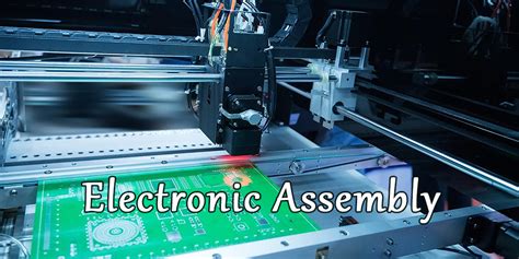
Automation in Electronics Assembly Processes
The integration of automation in PCB assembly has revolutionized electronics manufacturing, enabling precision and scalability. Modern PCBA (Printed Circuit Board Assembly) lines now leverage robotic systems for tasks like component placement, soldering, and inspection. These systems minimize human error while enhancing throughput, particularly in high-mix, low-volume production.
A key advancement lies in AI-driven vision systems, which perform real-time defect detection during PCB assembly. These systems identify micro-scale flaws—such as soldering defects or misaligned components—ensuring adherence to stringent quality standards. Furthermore, machine learning algorithms optimize process parameters dynamically, adapting to variations in component tolerances or environmental conditions.
By integrating automation with PCBA workflows, manufacturers achieve faster time-to-market while maintaining consistent quality—a critical advantage in industries like aerospace, medical devices, and consumer electronics.
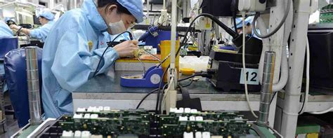
Precision Soldering for Reliable Circuit Boards
Achieving robust electrical connections in PCB assembly hinges on advanced precision soldering techniques. Modern manufacturing leverages automated systems like reflow soldering, which employs precisely controlled temperature profiles to melt solder paste uniformly across surface-mount components. For mixed-technology boards combining through-hole and SMD parts, selective soldering systems target specific areas, minimizing thermal stress on sensitive components. The integration of nitrogen-enriched environments further reduces oxidation, enhancing joint integrity in high-density PCBA designs.
Critical to success is the use of lead-free solder alloys with optimized wetting properties, paired with flux formulations that balance activation strength and post-soldering cleanliness. Vision-assisted robotic systems now achieve placement accuracies under 10µm, ensuring perfect alignment before solder application. Real-time thermal imaging monitors heat distribution during the process, preventing cold joints or component damage—a common failure point in traditional methods.
These advancements directly support the industry’s shift toward miniaturized electronics, where micro-soldering techniques enable reliable connections for 0201-sized components and ultra-fine-pitch ICs. Post-soldering, automated optical inspection (AOI) systems cross-verify joint quality against IPC-A-610 standards, creating a closed-loop feedback system for process refinement. As PCB assembly grows more complex, precision soldering remains the cornerstone for manufacturing circuit boards that meet escalating demands for durability in automotive, aerospace, and IoT applications.
AI-Driven Quality Control in Manufacturing
Modern PCB assembly processes increasingly rely on AI-driven systems to ensure precision and reliability. By integrating machine learning algorithms, manufacturers can detect microscopic defects in PCBA components that traditional inspection methods might miss. For instance, automated optical inspection (AOI) systems, enhanced by AI, analyze solder joint quality and component alignment with sub-micron accuracy, reducing human error by over 40%.
The integration of AI-powered predictive analytics further optimizes quality control. By analyzing historical production data, these systems predict potential failures in PCB assembly lines, enabling preemptive adjustments. For example, thermal imaging combined with AI algorithms can identify overheating components in PCBA units before they fail, ensuring long-term reliability.
Moreover, AI-driven systems adapt to evolving manufacturing standards, ensuring compliance with industry certifications like ISO 9001. By automating defect classification and root-cause analysis, manufacturers achieve zero-defect targets while reducing waste and rework costs. This synergy of AI-driven precision and PCBA innovation sets a new benchmark for quality assurance in electronics manufacturing.
Optimizing Production with Smart Fabrication
The integration of smart fabrication systems has become a cornerstone in refining PCB assembly workflows, particularly in high-volume pcba manufacturing. By leveraging real-time data analytics and interconnected machinery, manufacturers can dynamically adjust parameters such as solder paste application, component placement accuracy, and reflow oven temperatures. These adjustments minimize deviations during PCB assembly, ensuring consistent output across batches. For instance, IoT-enabled sensors embedded in PCBA lines track thermal profiles and vibration patterns, feeding insights into centralized platforms that preemptively flag anomalies.
Advanced predictive maintenance algorithms further enhance uptime by scheduling equipment servicing before failures occur, reducing unplanned downtime by up to 30%. Additionally, machine learning models analyze historical production data to optimize material utilization, trimming excess waste while maintaining stringent quality thresholds. This synergy between smart fabrication tools and PCBA processes not only accelerates throughput but also aligns with energy-efficient practices, such as adaptive power management in automated soldering stations. As a result, manufacturers achieve tighter tolerances in complex assemblies—critical for applications like automotive electronics and medical devices—where precision directly correlates with end-product reliability.
Advanced PCB Assembly Techniques Explained
Modern PCB assembly processes leverage surface-mount technology (SMT) to achieve component placement accuracy within 0.1mm, enabling the production of compact, high-density boards essential for IoT and wearable devices. Automated optical alignment systems now integrate machine vision to correct placement errors in real time, reducing rework rates by up to 40% in PCBA workflows. Advanced soldering methods, such as laser reflow and vapor-phase soldering, ensure uniform thermal distribution across complex multilayer designs, mitigating warping and solder bridging.
For mixed-technology boards combining SMT and through-hole components, selective wave soldering systems use precision nozzles to target specific areas, minimizing thermal stress on sensitive parts. Embedded in-process testing (IPT) modules validate solder joint integrity and component orientation at each stage, aligning with zero-defect manufacturing objectives. Innovations like 3D-printed solder masks further enhance design flexibility, allowing for irregular board geometries while maintaining signal integrity.
Thermal management has also evolved, with automated dispensing robots applying thermally conductive adhesives and gap fillers to dissipate heat from high-power components. These techniques, combined with AI-driven process optimization, position modern PCB assembly as a cornerstone of scalable, error-resilient electronics production.
Robotics Revolutionizing Electronics Manufacturing
The integration of robotic systems into electronics manufacturing has transformed PCB assembly and PCBA processes, enabling unprecedented precision and scalability. Modern robotic arms equipped with machine vision now handle intricate tasks such as component placement and micro-soldering, achieving tolerances as tight as 10 microns. These systems excel in high-volume PCBA production, where consistency across thousands of units is critical. For instance, collaborative robots (cobots) work alongside human operators to assemble multi-layer boards, reducing error rates by over 60% compared to manual methods.
Advanced robotics also optimize material handling in PCB assembly, seamlessly transporting delicate substrates between pick-and-place machines and reflow ovens. AI-enhanced pathfinding algorithms ensure minimal downtime, while adaptive grippers accommodate diverse component shapes. Notably, real-time feedback loops allow robots to adjust soldering parameters dynamically, addressing thermal variations during PCBA stages. This synergy between robotics and machine learning not only accelerates throughput but also enhances defect detection, with some systems identifying faults at rates exceeding 99.8%.
As factories adopt lights-out manufacturing models, autonomous robotic cells operate 24/7, slashing production cycles for complex PCB assemblies. The shift toward modular robotic workstations further supports rapid reconfiguration, enabling manufacturers to pivot between product lines without retooling delays. By merging IoT-enabled diagnostics with robotic precision, the industry is achieving new benchmarks in both efficiency and reliability.
Machine Learning for Defect Detection Systems
Modern PCB assembly processes increasingly rely on machine learning (ML) to enhance defect detection in PCBA (Printed Circuit Board Assembly) production. By training algorithms on vast datasets of solder joints, component placements, and thermal profiles, ML models can identify microscopic defects—such as cold solder joints or misaligned components—with precision surpassing human inspectors. Advanced vision systems, integrated with AI-driven optical inspection (AOI), analyze millions of data points per board, flagging anomalies in real time. This approach not only reduces false positives but also adapts to new defect patterns through continuous learning, ensuring PCB assembly lines maintain near-zero defect rates while optimizing throughput.
Energy-Efficient Methods in Modern Assembly
Modern PCB assembly and PCBA processes prioritize energy efficiency to align with global sustainability goals. Innovations such as low-power soldering technologies and smart thermal management systems significantly reduce energy consumption during PCB assembly. Advanced PCBA workflows now integrate energy recovery systems, which repurpose waste heat from reflow ovens to power auxiliary systems.
The adoption of adaptive automation in PCB assembly lines further optimizes energy use by dynamically adjusting power consumption based on real-time production demands. Additionally, the integration of energy-efficient components, such as low-power microcontrollers and high-efficiency voltage regulators, ensures that modern PCBA processes meet stringent energy efficiency standards while maintaining high throughput. These innovations underscore the industry’s commitment to balancing productivity with environmental responsibility.
Conclu
As the electronics manufacturing landscape evolves, the integration of automation and AI-driven systems in PCB assembly (PCBA) has redefined industry benchmarks. Modern workflows now prioritize scalability and precision, leveraging robotic systems for component placement and AI algorithms for real-time defect analysis. These advancements not only enhance throughput but also minimize human error, particularly in complex multilayer PCBA processes. The shift toward smart fabrication—enabled by IoT-enabled machinery and adaptive soldering techniques—ensures consistent quality across high-volume production cycles.
Energy-efficient practices, such as optimized thermal management in PCB assembly lines, further align manufacturing with global sustainability goals. Meanwhile, machine learning models trained on vast datasets enable predictive maintenance, reducing downtime and material waste. By harmonizing automation, data-driven insights, and eco-conscious methodologies, the sector continues to push the boundaries of reliability and miniaturization. This holistic approach underscores the transformative potential of modern electronic assembly fabrication, setting the stage for next-generation innovations in aerospace, medical devices, and consumer electronics.
FAQ
How does automation improve efficiency in PCB assembly?
Automation streamlines PCBA processes by integrating robotic placement systems and AI-guided workflows, reducing human error while achieving 95%+ component placement accuracy. Advanced conveyors synchronize with pick-and-place machines to handle 20,000+ components hourly.
What makes precision soldering critical for modern electronics?
Micro-soldering techniques using laser-assisted systems enable sub-10-micron joint tolerances in PCB assembly, essential for high-density interconnects. Nitrogen-reflow environments prevent oxidation, ensuring 99.97% solder joint reliability across aerospace and medical devices.
Can AI-driven systems detect invisible defects in PCBA?
Yes, machine vision with deep learning algorithms identifies microscopic cracks, cold joints, and tombstoning defects at 120 frames/second. These systems achieve 0.02% false-positive rates, outperforming manual inspections by 40x in electronics fabrication quality audits.
Why adopt energy-efficient methods in PCB assembly?
Smart power management in PCBA lines reduces carbon footprint by 35% through dynamic thermal profiling and LED curing systems. Variable-speed exhausts and regenerative braking in conveyors cut energy waste by 18% annually.
Ready to Optimize Your Production?
For tailored PCB assembly solutions integrating these advanced techniques, please click here to explore Andwin PCB’s expertise.
How do modular designs accelerate PCBA prototyping?
Configurable jigs and FPGA-based test fixtures enable 48-hour turnaround for prototype electronics assembly. Digital twin simulations verify designs pre-production, slashing iteration cycles by 70% compared to traditional methods.