Rapid PCB Prototyping: Revolutionizing Electronics Development
Introduction
In the fast-paced world of electronics, the ability to quickly design, test, and iterate on printed circuit boards (PCBs) is crucial for staying competitive. Rapid PCB prototyping has emerged as a game-changer, enabling engineers and designers to accelerate the development process, reduce costs, and bring innovative products to market faster than ever before. This article explores the concept of rapid PCB prototyping, its benefits, the technologies driving it, and its impact on the electronics industry.
What is Rapid PCB Prototyping?
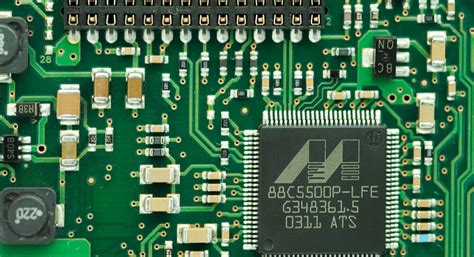
Rapid PCB prototyping refers to the process of quickly creating functional prototypes of printed circuit boards for testing and validation. Unlike traditional PCB manufacturing, which can take weeks or even months, rapid prototyping allows for the production of PCBs in a matter of days or even hours. This speed is achieved through the use of advanced manufacturing techniques, such as additive manufacturing, CNC milling, and advanced etching processes, combined with streamlined design and testing workflows.
The Importance of Rapid PCB Prototyping
- Accelerated Development Cycles: In the electronics industry, time-to-market is a critical factor. Rapid PCB prototyping allows companies to quickly iterate on designs, test new concepts, and refine their products. This acceleration in the development cycle can provide a significant competitive advantage, especially in industries where innovation is key.
- Cost Reduction: Traditional PCB manufacturing often involves high setup costs and long lead times, particularly for small production runs. Rapid prototyping reduces these costs by enabling the production of small batches of PCBs without the need for expensive tooling or lengthy setup processes. This cost efficiency is particularly beneficial for startups and small businesses with limited budgets.
- Improved Design Quality: Rapid prototyping allows engineers to test and validate their designs early in the development process. By identifying and addressing potential issues before mass production, companies can avoid costly redesigns and ensure that their final products meet the highest quality standards.
- Flexibility and Customization: Rapid PCB prototyping offers a high degree of flexibility, allowing designers to experiment with different layouts, materials, and components. This flexibility is particularly valuable in industries where customization and rapid adaptation to changing market demands are essential.
Technologies Driving Rapid PCB Prototyping
- Additive Manufacturing (3D Printing): Additive manufacturing, or 3D printing, has revolutionized the way PCBs are prototyped. By layering conductive and insulating materials, 3D printers can create complex PCB designs directly from digital files. This technology eliminates the need for traditional etching and drilling processes, significantly reducing production time and costs.
- CNC Milling: CNC (Computer Numerical Control) milling is another popular method for rapid PCB prototyping. CNC machines use precision cutting tools to remove material from a copper-clad board, creating the desired circuit pattern. This method is particularly useful for producing high-quality, single-layer or double-layer PCBs quickly.
- Advanced Etching Processes: Traditional etching processes involve the use of chemicals to remove unwanted copper from a PCB substrate. Rapid prototyping has seen the development of more advanced etching techniques, such as laser etching, which offers greater precision and faster turnaround times.
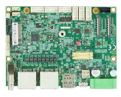
- Surface Mount Technology (SMT): SMT has become the standard for PCB assembly, allowing for the placement of components directly onto the surface of the board. Rapid prototyping often leverages SMT to quickly assemble and test PCBs, further reducing development time.
- Design Software and Simulation Tools: The availability of advanced PCB design software and simulation tools has greatly enhanced the rapid prototyping process. These tools allow designers to create and test virtual prototypes, identify potential issues, and optimize their designs before physical production begins.
The Rapid PCB Prototyping Process
- Design and Simulation: The rapid prototyping process begins with the creation of a digital design using PCB design software. Designers can use simulation tools to test the functionality of their circuits, identify potential issues, and optimize their designs.
- Prototype Fabrication: Once the design is finalized, the next step is to fabricate the physical prototype. Depending on the chosen method (e.g., 3D printing, CNC milling, or etching), the prototype can be produced in a matter of hours or days.
- Assembly and Testing: After fabrication, the PCB is assembled with the necessary components using SMT or through-hole technology. The assembled prototype is then tested to ensure that it functions as intended. Any issues identified during testing can be quickly addressed in the design phase.
- Iteration and Refinement: Rapid prototyping is an iterative process. Based on the results of testing, designers may need to make adjustments to the design and produce a new prototype. This cycle continues until the design meets all requirements and is ready for mass production.
Challenges and Considerations in Rapid PCB Prototyping
While rapid PCB prototyping offers numerous benefits, it also presents certain challenges that must be addressed to ensure success.
- Material Limitations: The materials used in rapid prototyping, particularly in 3D printing, may not always match the performance characteristics of traditional PCB materials. Designers must carefully consider the properties of the materials used and their impact on the final product.
- Precision and Accuracy: Achieving the necessary precision and accuracy in rapid prototyping can be challenging, especially for complex designs with fine features. Advanced manufacturing techniques and high-quality equipment are essential to meet these requirements.
- Cost vs. Speed Trade-offs: While rapid prototyping can reduce overall development costs, the initial investment in equipment and materials can be significant. Companies must carefully balance the need for speed with the associated costs.
- Scalability: Rapid prototyping is ideal for small-scale production and testing, but it may not always be suitable for large-scale manufacturing. Companies must consider how to transition from prototyping to mass production while maintaining quality and efficiency.
The Future of Rapid PCB Prototyping
As technology continues to advance, the future of rapid PCB prototyping looks promising. Emerging technologies, such as flexible and stretchable electronics, are pushing the boundaries of what is possible with PCBs. Rapid prototyping will play a crucial role in the development of these next-generation electronics, enabling designers to experiment with new materials and form factors.
Additionally, the integration of artificial intelligence (AI) and machine learning (ML) into the design and testing process is expected to further enhance the capabilities of rapid prototyping. AI-driven design tools can optimize PCB layouts, predict potential issues, and suggest improvements, reducing the need for manual intervention and accelerating the development cycle.
Conclusion
Rapid PCB prototyping has transformed the way electronics are developed, offering unprecedented speed, flexibility, and cost efficiency. By leveraging advanced manufacturing techniques and design tools, companies can bring innovative products to market faster than ever before. As technology continues to evolve, rapid prototyping will remain a critical enabler of innovation in the electronics industry, driving the development of new and exciting products that shape the future of technology.