Telecom PCB Assembly Techniques for Reliable Network Infrastructur
Key Takeaway
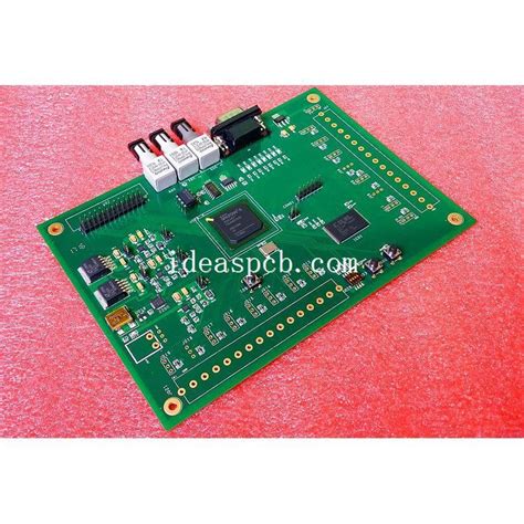
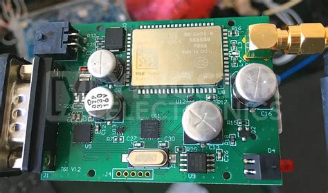
Modern PCB assembly processes form the backbone of resilient telecom infrastructure, particularly as 5G networks demand unprecedented precision. At the core of these systems lies PCBA (Printed Circuit Board Assembly), which integrates advanced manufacturing methods like laser-drilled microvias and multilayer stack-ups to minimize signal loss in high-frequency environments. Signal integrity remains a non-negotiable priority, achieved through impedance-controlled routing and EMI shielding techniques that safeguard data transmission across millimeter-wave spectrums. Equally critical is thermal management, where copper-core substrates and strategic component placement mitigate heat buildup in densely packed designs.
Automated testing protocols, including automated optical inspection (AOI) and X-ray verification, ensure defect-free PCB assembly outcomes, while material selection—such as low-loss laminates—optimizes performance under extreme operational stresses. For telecom providers, adopting these PCBA innovations not only elevates network reliability but also future-proofs infrastructure against evolving bandwidth demands. By balancing high-speed design principles with robust manufacturing standards, engineers can deliver 5G-ready solutions that maintain uptime in mission-critical applications.
Advanced PCB Manufacturing for 5G Networks
The transition to 5G networks demands unprecedented precision in PCB assembly, requiring materials and processes capable of handling millimeter-wave frequencies and ultra-low latency. Modern high-frequency laminates, such as Rogers 4350B or Taconic RF-35, are now standard in PCBA workflows to minimize signal loss at frequencies exceeding 28 GHz. Laser-drilled microvias and sequential lamination techniques enable multilayer designs that maintain impedance control while reducing crosstalk in densely packed telecom boards.
Tip: When selecting substrates for 5G PCB assembly, prioritize materials with a dielectric constant (Dk) below 3.0 and low dissipation factor (Df) to ensure minimal signal degradation at high speeds.
Advanced PCBA workflows integrate automated optical inspection (AOI) and 3D X-ray testing to detect micro-defects in ball grid arrays (BGAs) and quad flat no-lead (QFN) packages, which are critical for base station reliability. Additionally, embedded passive components and copper-filled via technology improve thermal dissipation, addressing the heat challenges posed by 5G’s higher power density. Manufacturers are also adopting hybrid rigid-flex PCB designs to accommodate compact antenna arrays and reduce interconnect losses in active antenna units (AAUs).
To support massive MIMO configurations, PCB assembly processes now emphasize tight tolerance controls for trace widths (±2%) and dielectric thickness (±5%), ensuring consistent performance across thousands of antenna elements. The use of lead-free solders with higher melting points further enhances long-term reliability in outdoor telecom environments.
Ensuring Signal Integrity in Telecom PCBs
Maintaining signal integrity is critical in high-frequency telecom PCB assembly, where even minor disruptions can degrade network performance. As 5G infrastructure demands faster data rates and lower latency, PCBA designs must address challenges like crosstalk, impedance mismatches, and electromagnetic interference (EMI). Advanced techniques such as controlled impedance routing and differential pair alignment are employed to preserve signal quality across multi-layer boards.
| Technique | Function | Impact on Signal Integrity |
|---|---|---|
| Ground Plane Shielding | Reduces EMI leakage | Improves noise immunity by 40-60% |
| Microstrip Line Design | Controls impedance fluctuations | Minimizes signal reflection |
| Via Optimization | Shortens return current paths | Lowers insertion loss by 15-20% |
In PCB assembly workflows, material selection directly influences signal attenuation. High-frequency laminates like Rogers 4350B are increasingly integrated into PCBA processes for their stable dielectric constants, particularly in mmWave applications. Simultaneously, automated optical inspection (AOI) systems verify trace geometries post-assembly, ensuring compliance with <3% impedance tolerance thresholds. These strategies collectively enable telecom infrastructure to handle 25 Gbps+ data transfers while maintaining bit error rates below 10⁻¹².
Thermal Management Solutions for Reliable PCBs
Effective thermal management is critical in PCB assembly for telecom applications, where high-power components and dense circuitry demand precise heat dissipation strategies. In 5G infrastructure, thermal vias, metal-core substrates, and advanced PCBA techniques work synergistically to mitigate thermal stress. For instance, copper-filled vias and aluminum-backed laminates enhance heat transfer away from sensitive components, ensuring operational stability in base stations and routers. Engineers also prioritize thermal interface materials (TIMs) with high conductivity ratings to bridge gaps between heat-generating ICs and cooling solutions.
Modern PCB assembly workflows integrate real-time thermal simulations during design, allowing optimization of component placement and airflow patterns. Liquid cooling systems, though less common in traditional telecom PCBA, are gaining traction for high-frequency mmWave applications where localized hotspots threaten signal integrity. Additionally, automated optical inspection (AOI) systems now incorporate infrared imaging to detect thermal anomalies during quality assurance, aligning with industry demands for zero-defect manufacturing.
As networks evolve toward higher power densities, material selection becomes pivotal. Ceramic-filled substrates and low-CTE dielectrics in PCBA processes reduce warping risks under thermal cycling, directly supporting infrastructure longevity. These solutions not only address immediate heat challenges but also future-proof designs against escalating performance requirements in next-gen telecom systems.
High-Speed PCB Design Best Practices
Achieving optimal performance in telecom PCB assembly demands meticulous attention to high-frequency signal propagation and impedance control. A critical step involves implementing controlled impedance routing to minimize signal loss, particularly in multi-layered boards handling 5G millimeter-wave frequencies. Designers must prioritize dielectric material selection, opting for low-loss substrates like Rogers or Isola laminates, which maintain stable electrical properties under thermal stress.
To mitigate crosstalk and electromagnetic interference (EMI), differential pair routing with precise spacing and length matching is essential. Advanced PCBA workflows integrate simulation tools to validate signal integrity pre-fabrication, reducing post-production rework. Thermal management strategies, such as embedding thermal vias near high-power components, prevent localized overheating that could degrade signal paths.
Layer stack-up optimization further enhances performance—placing high-speed traces on inner layers shielded by ground planes minimizes noise coupling. For edge-rate-sensitive applications, termination resistors and guard traces are employed to dampen reflections. Collaboration between PCB assembly teams and design engineers ensures manufacturability, balancing tight tolerances with cost-effective production. By adhering to these practices, telecom infrastructure gains the reliability needed to support next-generation networks.
Automated Testing in Telecom PCB Assembly
As telecom networks evolve to support 5G and beyond, PCB assembly processes demand unprecedented precision to maintain signal integrity and operational stability. Automated testing has emerged as a cornerstone of modern PCBA manufacturing, enabling rapid validation of high-density boards while minimizing human error. Advanced systems leverage automated optical inspection (AOI) to detect micro-scale defects in solder joints and component alignment, while X-ray testing ensures the integrity of hidden connections in multilayer designs. For high-frequency applications, in-circuit testing (ICT) verifies electrical performance under simulated network loads, identifying impedance mismatches or crosstalk that could degrade signal quality.
Transitioning from prototype to mass production, automated protocols streamline stress testing for thermal resilience, a critical factor in outdoor telecom infrastructure. By integrating machine learning algorithms, test systems adapt to evolving PCB assembly standards, flagging anomalies in real time and reducing time-to-market for 5G-ready hardware. This approach not only aligns with the zero-defect targets of telecom operators but also supports scalable quality control across global supply chains. As component miniaturization intensifies, the synergy between PCBA automation and AI-driven analytics will remain pivotal in safeguarding network uptime and future-proofing critical communication ecosystems.
Optimizing PCB Materials for Network Reliability
Selecting optimal materials for PCB assembly is critical to maintaining network reliability in telecom systems. High-frequency laminates, such as Rogers or PTFE-based substrates, are increasingly prioritized in PCBA designs to minimize signal loss at 5G frequencies. These materials offer low dielectric constants (Dk) and dissipation factors (Df), ensuring stable performance in high-speed data transmission. For thermal resilience, metal-core or ceramic-filled laminates are integrated to dissipate heat efficiently, reducing the risk of component degradation in densely packed telecom infrastructure.
Material compatibility with automated assembly processes also plays a role in reliability. Halogen-free laminates, for instance, meet environmental regulations while maintaining mechanical stability during PCB assembly. Advanced coatings like conductive anodic filament (CAF)-resistant finishes further prevent electrochemical migration in humid conditions. By pairing these materials with high-density interconnect (HDI) layouts, manufacturers achieve tighter signal routing without compromising structural integrity.
Transitioning to next-gen networks demands rigorous material validation. PCBA teams employ thermal cycling tests and accelerated life testing to simulate decades of operation, ensuring substrates withstand thermal expansion mismatches. This proactive approach aligns with the broader focus on future-proofing telecom infrastructure, where material choices directly impact long-term network uptime and maintenance costs.
Future-Proofing Telecom Infrastructure With PCBs
Telecom infrastructure demands PCB assembly processes that anticipate evolving network requirements while maintaining backward compatibility. As 5G deployments expand and IoT ecosystems grow, engineers are adopting modular design principles in PCBA workflows to enable seamless hardware upgrades without full system overhauls. This approach integrates high-speed materials like PTFE-based laminates and low-loss prepregs, which support millimeter-wave frequencies while minimizing signal attenuation in legacy networks.
A critical strategy involves embedding field-programmable gate arrays (FPGAs) within multilayer boards, allowing remote reconfiguration of signal routing protocols as bandwidth demands escalate. Advanced thermal management techniques—such as copper-filled microvias and thermally conductive dielectric layers—are being standardized to handle increased power densities in compact 5G node installations.
Leading manufacturers now implement predictive maintenance algorithms through PCB assembly test points, analyzing real-time impedance variations to flag potential failures before service disruptions occur. By combining high-density interconnect (HDI) layouts with hybrid rigid-flex constructions, modern PCBA techniques achieve 40% greater component density than conventional designs, crucial for space-constrained urban microcells.
The industry is shifting toward open radio access network (O-RAN) compatible architectures in PCB assembly, using standardized interfaces that allow multi-vendor hardware interoperability. This paradigm, supported by AI-driven signal integrity simulations during the PCBA design phase, ensures telecom carriers can integrate emerging technologies like terahertz backhaul systems without complete infrastructure replacements.
5G-Ready PCB Assembly Techniques Explai
Achieving 5G-ready PCB assembly demands precision engineering to address the unique challenges of high-frequency signal transmission and dense component integration. Central to this process is the implementation of impedance-controlled routing, which minimizes signal loss and maintains integrity across millimeter-wave frequencies. Advanced PCBA workflows now incorporate low-loss dielectric materials like Rogers 4350B, optimized for RF performance in telecom infrastructure.
To ensure compatibility with 5G’s stringent latency requirements, manufacturers employ laser-drilled microvias and sequential lamination techniques, enabling multilayer designs with reduced parasitic capacitance. Thermal management is enhanced through embedded copper coin technology, which directs heat away from power amplifiers and baseband processors—critical for maintaining network reliability in 24/7 operation.
Modern telecom PCB assembly also integrates automated optical inspection (AOI) systems paired with boundary-scan testing, verifying signal paths in complex array architectures. The use of surface-mount device (SMD) shielding further mitigates electromagnetic interference, a non-negotiable factor in multi-antenna 5G systems. By combining these techniques with design-for-manufacturing (DFM) principles, PCBA specialists create boards that meet both current 5G standards and future scalability demands.
Conclu
The evolution of PCB assembly methodologies has become a cornerstone in building resilient telecom infrastructure, particularly as 5G deployments demand unprecedented precision. By integrating high-speed design principles with PCBA processes optimized for signal fidelity, manufacturers can mitigate latency and electromagnetic interference—critical factors in maintaining network uptime. Equally vital are thermal management strategies, which ensure long-term reliability by dissipating heat efficiently in densely packed telecom equipment.
Advancements in automated testing protocols further refine PCB assembly workflows, enabling rapid identification of defects while adhering to stringent quality benchmarks. Material selection, such as high-frequency laminates and low-loss substrates, plays a pivotal role in sustaining signal integrity across millimeter-wave applications. As networks scale, the synergy between PCBA innovations and modular design philosophies allows infrastructure to adapt seamlessly to evolving standards.
Looking ahead, the telecom sector’s reliance on robust PCB assembly techniques will only intensify. By prioritizing future-ready manufacturing frameworks and cross-disciplinary collaboration, stakeholders can ensure that next-generation networks deliver both performance and durability, meeting the dynamic demands of global connectivity.
FAQ
What distinguishes standard PCB assembly from telecom-specific PCBA processes?
Telecom PCBA requires military-grade precision to handle high-frequency signals and extreme thermal cycles. Unlike consumer electronics, these assemblies undergo automated optical inspection (AOI) and X-ray testing to meet 5G latency standards below 1ms.
How do thermal challenges impact PCB assembly reliability in 5G base stations?
5G infrastructure generates up to 40% more heat than 4G systems. Advanced PCBA integrates copper-core substrates and thermal vias to dissipate 150W/cm² heat loads, preventing signal degradation in millimeter-wave frequencies.
Why is material selection critical for PCB assembly in network reliability?
High-speed PTFE laminates with Dk values under 3.0 minimize signal loss above 10GHz. Telecom-grade PCBAs pair these with low-loss solder masks to maintain impedance stability across 10,000+ thermal cycles.
Can existing PCB assembly lines support 6G-ready infrastructure?
While current PCBA processes handle 28GHz 5G bands, 6G’s terahertz frequencies require substrate-integrated waveguides and laser-drilled microvias. Forward-looking manufacturers are adopting hybrid HDI-SLPTM techniques for seamless upgrades.
Ready to Optimize Your Telecom PCB Assembly?
For expert-level PCBA solutions tailored to 5G/6G demands, please click here to explore Andwin PCB’s ISO-certified assembly services.