Custom Printed Circuit Boards: Design, Manufacturing, and Applications
Introduction
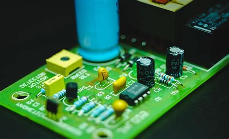
Printed Circuit Boards (PCBs) are the backbone of modern electronics. They provide the physical platform for mounting and interconnecting electronic components, enabling the functionality of devices ranging from smartphones to industrial machinery. While standard PCBs are widely available and suitable for many applications, custom printed circuit boards offer tailored solutions for specialized needs. This article explores the design, manufacturing, and applications of custom PCBs, highlighting their importance in today’s technology-driven world.
1. Understanding Custom Printed Circuit Boards
Custom PCBs are designed and manufactured to meet specific requirements that standard off-the-shelf PCBs cannot fulfill. These requirements may include unique shapes, sizes, layer counts, materials, or specific electrical and thermal properties. Custom PCBs are essential for applications where performance, reliability, and space constraints are critical.
1.1. Key Features of Custom PCBs
- Tailored Design: Custom PCBs are designed to fit specific applications, ensuring optimal performance and compatibility with other components.
- Flexibility: They can be made in various shapes and sizes, including rigid, flexible, and rigid-flex configurations.
- Advanced Materials: Custom PCBs can utilize specialized materials such as high-frequency laminates, metal-core substrates, or high-temperature resins.
- Complex Layouts: They support intricate routing and high-density interconnects, accommodating complex circuits in compact spaces.
2. Design Process of Custom PCBs
The design of custom PCBs is a meticulous process that involves several stages, from conceptualization to final layout. Each stage requires careful consideration to ensure the PCB meets the desired specifications and performance criteria.
2.1. Requirement Analysis
The first step in designing a custom PCB is to understand the application’s requirements. This includes:
- Functional Requirements: What the PCB needs to achieve, such as signal processing, power distribution, or data communication.
- Environmental Conditions: Operating temperature, humidity, vibration, and exposure to chemicals or radiation.
- Mechanical Constraints: Size, shape, and mounting requirements.
- Electrical Specifications: Voltage, current, signal integrity, and electromagnetic compatibility (EMC).
2.2. Schematic Design
Once the requirements are clear, the next step is to create a schematic diagram. This diagram represents the electrical connections between components and serves as a blueprint for the PCB layout.
- Component Selection: Choosing the right components based on performance, availability, and cost.
- Circuit Design: Defining the electrical connections and ensuring the circuit meets the functional requirements.
- Simulation: Using software tools to simulate the circuit’s behavior and identify potential issues before moving to the layout stage.
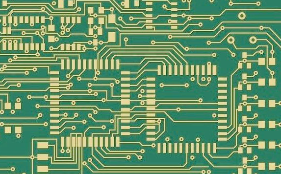
2.3. PCB Layout
The PCB layout is where the schematic is translated into a physical design. This stage involves placing components and routing traces on the board.
- Component Placement: Arranging components to optimize signal flow, minimize noise, and ensure efficient heat dissipation.
- Routing: Connecting components with copper traces, considering factors like signal integrity, impedance matching, and crosstalk.
- Layer Stackup: Determining the number of layers and their arrangement to meet electrical and mechanical requirements.
- Design Rule Check (DRC): Verifying the layout against design rules to ensure manufacturability and reliability.
2.4. Prototyping and Testing
After the layout is finalized, a prototype is manufactured to validate the design.
- Prototype Fabrication: Producing a small batch of PCBs for testing.
- Functional Testing: Verifying that the PCB performs as intended under real-world conditions.
- Debugging: Identifying and fixing any issues that arise during testing.
- Iteration: Refining the design based on test results and feedback.
3. Manufacturing Process of Custom PCBs
The manufacturing of custom PCBs involves several precise steps to transform the design into a functional board. The process varies depending on the complexity of the PCB and the materials used.
3.1. Material Selection
The choice of materials is critical to the performance and durability of the PCB.
- Substrate: Typically made of fiberglass (FR4), but can also be ceramic, metal-core, or flexible materials like polyimide.
- Copper: Used for conductive traces, with thicknesses ranging from 1 oz to 3 oz or more.
- Solder Mask: A protective layer that prevents solder bridges and provides insulation.
- Silkscreen: Used for labeling components and providing assembly instructions.
3.2. Layer Preparation
For multi-layer PCBs, each layer is prepared individually.
- Inner Layers: Copper-clad laminates are etched to form the inner circuit patterns.
- Lamination: Layers are stacked and bonded together under heat and pressure.
- Drilling: Holes are drilled for vias and component leads.
- Plating: Holes are plated with copper to establish electrical connections between layers.
3.3. Outer Layer Processing
The outer layers undergo additional processing to complete the PCB.
- Imaging: A photoresist is applied and exposed to UV light to transfer the circuit pattern.
- Etching: Unwanted copper is removed, leaving behind the desired traces.
- Solder Mask Application: A solder mask is applied and cured to protect the traces.
- Surface Finish: A surface finish (e.g., HASL, ENIG, OSP) is applied to protect the copper and facilitate soldering.
3.4. Testing and Inspection
Before the PCBs are shipped, they undergo rigorous testing and inspection.
- Electrical Testing: Verifying continuity and isolation of circuits.
- Automated Optical Inspection (AOI): Checking for defects in the solder mask, traces, and components.
- X-Ray Inspection: Inspecting internal layers and vias for defects.
- Functional Testing: Ensuring the PCB performs as intended.
4. Applications of Custom Printed Circuit Boards
Custom PCBs are used in a wide range of industries and applications, each with its own unique requirements.
4.1. Consumer Electronics
- Smartphones and Tablets: Custom PCBs enable compact, high-performance designs with advanced features like 5G connectivity and high-resolution displays.
- Wearable Devices: Flexible and rigid-flex PCBs are used in smartwatches, fitness trackers, and medical wearables.
4.2. Automotive
- Engine Control Units (ECUs): Custom PCBs manage engine performance, fuel efficiency, and emissions.
- Advanced Driver-Assistance Systems (ADAS): High-reliability PCBs are essential for safety-critical systems like collision avoidance and lane-keeping assist.
4.3. Industrial Automation
- Programmable Logic Controllers (PLCs): Custom PCBs provide the processing power and connectivity needed for industrial control systems.
- Robotics: High-density PCBs with robust thermal management are used in robotic arms and autonomous vehicles.
4.4. Medical Devices
- Imaging Equipment: Custom PCBs are used in MRI machines, X-ray systems, and ultrasound devices.
- Implantable Devices: Biocompatible materials and miniaturized designs are critical for pacemakers and neurostimulators.
4.5. Aerospace and Defense
- Avionics: Custom PCBs must withstand extreme temperatures, vibrations, and radiation in aircraft and spacecraft.
- Military Communications: High-frequency PCBs are used in radar systems, satellite communications, and encrypted networks.
5. Challenges and Future Trends
While custom PCBs offer numerous advantages, they also present challenges that must be addressed to meet the demands of emerging technologies.
5.1. Challenges
- Complexity: As devices become more advanced, PCBs must accommodate higher component densities and more intricate routing.
- Thermal Management: High-power applications require effective heat dissipation to prevent component failure.
- Signal Integrity: Maintaining signal integrity at high frequencies is critical for performance and reliability.
- Cost: Custom PCBs can be more expensive than standard ones, especially for low-volume production.
5.2. Future Trends
- Miniaturization: The trend towards smaller, more compact devices will drive the development of high-density interconnect (HDI) PCBs.
- Flexible and Stretchable PCBs: Emerging technologies like foldable smartphones and wearable electronics will increase demand for flexible and stretchable PCBs.
- Advanced Materials: The use of new materials, such as graphene and carbon nanotubes, could revolutionize PCB performance.
- Sustainability: Eco-friendly materials and manufacturing processes will become increasingly important as the industry moves towards sustainability.
Conclusion
Custom printed circuit boards are essential for meeting the unique requirements of modern electronic devices. From design and manufacturing to application, custom PCBs offer unparalleled flexibility and performance. As technology continues to evolve, the demand for custom PCBs will only grow, driving innovation and pushing the boundaries of what is possible in electronics. Whether in consumer electronics, automotive, industrial automation, medical devices, or aerospace, custom PCBs will remain at the heart of technological advancement.