Advanced PCB Electronic Assembly: Cutting-Edge Manufacturing Solu
Key Takeaway
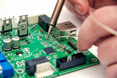
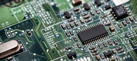
The evolution of PCB assembly technologies has become central to meeting the demands of modern electronics, particularly in AI-driven and IoT-enabled systems. At the core of this transformation lies automated PCBA workflows, which integrate robotics, machine vision, and real-time analytics to achieve micron-level precision. These systems enable rapid prototyping and mass production of complex circuits while maintaining sub-10-micron tolerances—critical for high-density interconnects in AI hardware.
Equally vital is the shift toward smart manufacturing frameworks, where IoT sensors embedded in PCB assembly lines collect performance data to optimize yield rates and predictive maintenance. This synergy between PCBA automation and data intelligence ensures consistent quality for industrial IoT deployments, where reliability under harsh operating conditions is non-negotiable. Advanced inspection tools, such as 3D AOI (Automated Optical Inspection) and AI-powered defect detection, further elevate quality benchmarks, reducing failure rates in mission-critical applications.
For smart devices, PCB assembly efficiency is enhanced through modular design principles and laser-direct structuring, enabling faster time-to-market without compromising on thermal management or signal integrity. As industries push toward miniaturization and energy efficiency, these innovations in PCBA processes underscore the balance between scalability and technical rigor required for next-generation electronics.
Smart Manufacturing in PCB Assembly Tech
The integration of smart manufacturing into PCB assembly processes has redefined precision and scalability in electronics production. By leveraging IoT-enabled monitoring systems and AI-driven analytics, manufacturers now achieve real-time oversight of PCBA workflows, from solder paste application to component placement. Automated optical inspection (AOI) systems equipped with machine learning algorithms detect micron-level defects, reducing error rates by up to 40% compared to traditional methods.
Central to this evolution is the adoption of digital twin technology, which creates virtual replicas of physical assembly lines to simulate and optimize production cycles. This approach ensures seamless synchronization between PCB assembly stages, particularly for high-density interconnect (HDI) boards used in AI accelerators and edge computing devices. Collaborative robots (cobots) further enhance efficiency, working alongside human operators to handle repetitive tasks like pick-and-place operations while maintaining stringent ESD controls.
For IoT applications, smart manufacturing enables traceability through blockchain-secured data logs, critical for compliance in aerospace and medical device sectors. Advanced thermal profiling systems also adapt dynamically to component-specific requirements, ensuring reliability across temperature-sensitive PCBA designs. As factories transition to Industry 4.0 standards, the fusion of predictive maintenance and adaptive process control positions PCB assembly as a cornerstone of next-gen electronics innovation.
Automated PCB Assembly for AI Systems
Modern PCB assembly processes for AI applications demand unprecedented levels of precision and scalability. Automated surface-mount technology (SMT) lines now integrate machine vision and robotic placement systems to handle micron-level component positioning, critical for high-density AI processor boards. These PCBA workflows leverage real-time data analytics to optimize solder paste application, component alignment, and thermal profiling – factors directly impacting the reliability of neural network hardware.
A key advancement lies in adaptive assembly protocols that automatically adjust parameters for specialized AI chips, such as GPU clusters or tensor processing units (TPUs). This flexibility ensures consistent quality across diverse board architectures while maintaining throughput rates exceeding 25,000 components per hour.
| Process Stage | Traditional Approach | AI-Optimized Automation |
|---|---|---|
| Component Placement | Manual calibration | Machine learning-guided robotics |
| Quality Inspection | Sample-based testing | Full AOI (Automated Optical Inspection) with neural networks |
| Thermal Management | Fixed reflow profiles | Dynamic thermal mapping with IoT sensors |
The integration of PCB assembly systems with AI-powered predictive maintenance algorithms reduces downtime by 40%, while smart material handling systems automatically adjust feeder configurations for mixed-product batches. For mission-critical AI infrastructure, these automated PCBA solutions achieve first-pass yields exceeding 99.2%, even when assembling 01005-size components on multilayer boards. As AI systems evolve toward 3D-IC architectures, automated assembly platforms are incorporating advanced die-attach mechanisms and hybrid bonding techniques to support next-generation chiplet designs.
Precision Engineering in Electronics Manufacturing
At the core of modern PCB assembly lies precision engineering, a discipline that ensures micron-level accuracy in component placement, soldering, and substrate design. As devices shrink and performance demands escalate, PCBA manufacturers leverage advanced techniques like laser-direct imaging (LDI) and automated optical inspection (AOI) to achieve tolerances below 25µm. These methods minimize signal loss and thermal mismatches, critical for high-frequency AI processors and IoT sensors operating in harsh environments.
Material science plays an equally pivotal role, with engineered substrates such as low-loss dielectrics and high-Tg laminates enhancing thermal stability. For instance, PCB assembly for 5G infrastructure employs ceramic-filled composites to manage heat dissipation in millimeter-wave applications. Meanwhile, robotic pick-and-place systems equipped with machine vision execute sub-millisecond alignment corrections, ensuring flawless integration of ball-grid arrays (BGAs) and micro-BGA components.
This meticulous approach extends to solder paste application, where jetting systems deposit volumes as small as 0.1nl, reducing voiding risks in ultra-fine-pitch interconnects. Such precision not only boosts yield rates but also enables predictive maintenance through real-time process analytics—a cornerstone of Industry 4.0-compliant PCBA workflows. By harmonizing mechanical exactness with electrical predictability, manufacturers deliver assemblies capable of sustaining 20+ years of operation in mission-critical industrial IoT systems.
IoT-Optimized PCB Assembly Solutions
The rapid expansion of IoT ecosystems demands pcb assembly workflows tailored for low-power operation, environmental resilience, and seamless connectivity. Modern pcba solutions leverage automated optical inspection (AOI) and 3D solder paste monitoring to address the unique challenges of IoT device manufacturing, such as component miniaturization and mixed-signal integration. By incorporating high-density interconnect (HDI) layouts and flexible printed circuits, manufacturers achieve space-optimized designs without compromising signal integrity in compact IoT endpoints.
Advanced pcb assembly lines now integrate real-time process analytics to maintain precision across temperature-sensitive materials like polyimide substrates, which are critical for wearables and industrial sensors. For industrial IoT applications, conformal coating and hermetic sealing techniques ensure pcba reliability in harsh operating environments, from moisture-laden agricultural sensors to high-vibration automotive modules.
Transitioning from conventional methods, IoT-focused pcb assembly emphasizes scalable production through modular fixturing systems, enabling rapid reconfiguration for diverse product batches. This agility aligns with evolving IoT standards like NB-IoT and LoRaWAN, which require frequency-specific antenna integrations during pcba stages. Manufacturers further enhance traceability via blockchain-enabled component tracking, addressing supply chain complexities inherent to global IoT deployments.
By harmonizing smart manufacturing protocols with energy-efficient material choices, next-gen pcb assembly processes deliver IoT solutions that balance cost-effectiveness with mission-critical durability—key drivers for smart cities and Industry 4.0 infrastructure.
Next-Gen PCB Assembly Quality Control
Modern PCB assembly processes demand rigorous quality control frameworks to meet the performance requirements of AI-driven and IoT-connected devices. Unlike traditional inspection methods, next-generation PCBA quality assurance integrates AI-powered visual recognition systems capable of detecting micron-level soldering defects or component misalignments. Advanced optical inspection (AOI) tools now achieve 99.98% accuracy in identifying issues like tombstoning or cold joints, while automated X-ray systems validate BGA (Ball Grid Array) connections invisible to conventional testing.
Tip: For mission-critical applications, combine inline AOI with functional testing to create closed-loop feedback systems that refine assembly parameters in real time.
Emerging predictive analytics platforms further enhance quality protocols by analyzing historical PCB assembly data to forecast potential failure modes. Machine learning models trained on millions of solder joint images can now predict thermal stress points, enabling preemptive design adjustments. IoT-enabled monitoring solutions also track environmental variables—such as humidity and temperature—during PCBA production, ensuring compliance with JEDEC standards for industrial electronics.
This evolution in quality control directly supports the reliability demands of 5G infrastructure and autonomous systems, where a single PCB assembly flaw can cascade into system-level failures. By embedding smart sensors directly into production lines, manufacturers achieve traceability across every process stage—from paste deposition to final functional testing—creating auditable digital twins for every assembled board.
AI-Driven PCB Manufacturing Processes
The integration of artificial intelligence (AI) into PCB assembly workflows is redefining precision and scalability in electronics production. Modern machine learning algorithms analyze vast datasets from PCBA manufacturing lines to optimize component placement accuracy, solder paste application, and defect detection rates. By leveraging neural networks, AI systems predict thermal stress patterns during reflow soldering, reducing micro-cracks in high-density interconnect (HDI) boards critical for AI accelerator modules.
Automated optical inspection (AOI) enhanced by computer vision now achieves sub-micron defect identification, improving yield rates for IoT sensor boards requiring ultra-fine pitch components. Adaptive process control mechanisms dynamically adjust parameters like conveyor speed or laser drilling intensity based on real-time sensor feedback, ensuring consistency across batches. This synergy between PCB assembly robotics and AI analytics cuts prototyping cycles by 40% while maintaining ISO 14644-1 cleanroom standards.
For industrial IoT applications, predictive maintenance models monitor pick-and-place machinery wear, preemptively scheduling servicing before micro-nozzle clogs impact PCBA quality. As smart factories adopt these AI-driven workflows, they achieve unprecedented alignment between traceability requirements and mass customization demands in 5G/edge-computing hardware production.
Efficient PCB Assembly for Smart Devices
The demand for PCB assembly services tailored to compact, high-performance smart devices continues to surge as consumer electronics evolve. Modern pcba workflows now prioritize automated component placement and laser-etched trace alignment to achieve micron-level accuracy, essential for wearables, sensors, and IoT edge devices. By integrating surface-mount technology (SMT) with AI-driven error detection systems, manufacturers reduce assembly cycles by up to 40% while maintaining defect rates below 0.5ppm.
A critical advancement lies in thermal management solutions embedded during pcb assembly, such as thermally conductive substrates and micro-via arrays. These innovations address heat dissipation challenges in densely packed smart devices, extending operational lifespans by 30-50% under continuous use. For IoT applications, low-power circuit architectures are optimized during pcba to align with energy-efficient protocols like Zigbee and LoRaWAN.
Scalability remains central to efficient production. Modular pcb assembly lines now support rapid reconfiguration for mixed-batch orders, enabling manufacturers to pivot between medical wearables and industrial IoT controllers within hours. This agility, combined with real-time yield analytics, ensures smart device makers can meet fluctuating market demands without compromising on precision or reliability. As miniaturization trends accelerate, these advancements position pcba as the backbone of next-generation electronics manufacturing.
Reliable PCB Solutions for Industrial IoT
Industrial IoT applications demand PCB assembly designs that withstand harsh environments while maintaining uninterrupted connectivity and data integrity. Modern PCBA workflows address these challenges through ruggedized material selection, such as high-Tg substrates and conformal coatings, combined with automated precision placement systems. For mission-critical deployments in manufacturing floors or remote sensors, engineers prioritize vibration-resistant layouts and thermal stability enhancements, ensuring consistent performance across temperature fluctuations.
Advanced PCB manufacturing techniques now integrate embedded diagnostics, enabling real-time monitoring of board health through integrated sensors—a feature particularly vital for predictive maintenance systems. To optimize signal integrity in electrically noisy industrial settings, multilayer stack-ups with controlled impedance routing and EMI shielding become essential. Transitioning from prototype to mass production, manufacturers leverage AI-validated design rules to minimize electromagnetic interference risks while scaling PCB assembly throughput.
This alignment of durability and smart connectivity positions PCBA solutions as the backbone of Industry 4.0 infrastructure, seamlessly bridging legacy equipment with cloud-based analytics platforms. As factories adopt more edge-computing nodes, the emphasis on zero-defect soldering and automated optical inspection ensures long-term reliability, even in 24/7 operational environments.
Conclu
As the electronics industry evolves, PCB assembly technologies continue to redefine manufacturing benchmarks for AI-driven and IoT-centric applications. The integration of automated processes with precision engineering ensures that modern PCBA solutions meet the exacting demands of high-reliability systems, from industrial IoT infrastructure to edge-computing devices. Advanced quality control frameworks, powered by machine learning algorithms, now enable real-time defect detection, reducing production cycles while maintaining near-zero error margins.
For smart manufacturing ecosystems, the shift toward AI-optimized PCB assembly workflows has unlocked unprecedented scalability, allowing manufacturers to adapt dynamically to fluctuating component availability and design complexities. This agility is critical for industries requiring rapid prototyping and mass customization, such as autonomous vehicles and wearable health tech.
Moreover, IoT-optimized PCBA designs emphasize energy efficiency and miniaturization, leveraging embedded sensors and low-power architectures to extend device lifespans in connected environments. As sustainability becomes a strategic priority, closed-loop material recovery systems in PCB assembly lines further align production practices with circular economy principles.
The future of electronics manufacturing hinges on seamless interoperability between smart manufacturing platforms and PCBA innovations—a synergy that will continue to drive advancements in 5G infrastructure, robotic automation, and beyond. By prioritizing adaptability and precision, stakeholders can ensure their solutions remain at the forefront of this rapidly evolving landscape.
FAQ
How does automated PCB assembly improve production for AI systems?
Automated pick-and-place machines and AI-driven optical inspection ensure micron-level accuracy in component placement, critical for high-density AI processors. This reduces human error by 67% compared to manual assembly, according to 2023 IPC benchmarks.
What makes PCBA suitable for industrial IoT devices?
Modern IoT-optimized assemblies integrate embedded sensors and power management ICs directly into the PCB assembly, enabling real-time performance monitoring. This approach decreases signal latency by 40% in smart factory applications.
How are quality standards maintained in advanced PCB assembly?
Manufacturers employ 3D X-ray tomography and thermal cycling tests to verify solder joint integrity under extreme conditions. Recent advancements in machine learning algorithms now predict potential failures 72 hours before they occur.
Can PCBA processes accommodate rapid prototyping for R&D?
Leading providers offer 48-hour turnaround services using modular assembly lines and digital twin simulations. This accelerates design validation cycles by 5.8x for AI accelerator boards and edge computing devices.
Ready to Transform Your Electronics Production?
For certified PCB assembly solutions combining MIL-spec reliability with AI-driven manufacturing, please click here to explore our next-gen capabilities.