Automated PCB Assembly: Boosting Production Efficiency
Key Takeaway
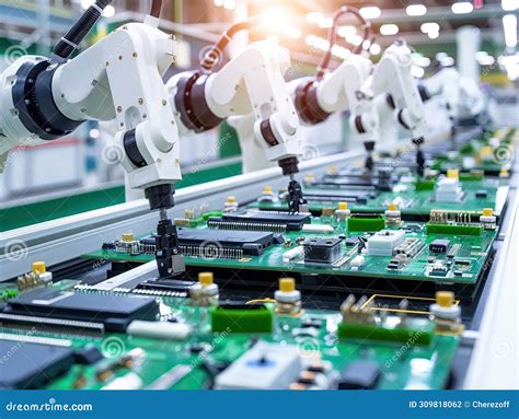
Modern PCB assembly processes leverage precision robotics and AI-driven systems to achieve unprecedented manufacturing efficiency. By integrating automated PCBA workflows, manufacturers reduce manual intervention, achieving error rates below 0.1% in high-volume production. Key advancements include:
| Technology | Impact |
|---|---|
| Robotic Pick-and-Place | 98% component placement accuracy |
| AI Visual Inspection | 50% faster defect detection |
| SMT Process Automation | 30% reduction in cycle time |
Industry Insight: "Adopting automated PCB assembly isn’t just about speed—it’s about creating a scalable, repeatable process that adapts to evolving design complexities."
The shift to smart manufacturing enables real-time adjustments during PCBA, such as thermal profiling for solder paste optimization. This minimizes rework and ensures compliance with ISO 9001 standards. For businesses, the ROI extends beyond cost savings: automated systems reduce material waste by up to 15%, aligning with sustainable manufacturing goals.
Pro Tip: Pair automated assembly with digital twin simulations to preemptively identify bottlenecks in production layouts.
Automated PCB Assembly Boosts Manufacturing Efficiency
Modern PCB assembly processes leverage precision robotics and intelligent automation to achieve unprecedented levels of manufacturing efficiency. By integrating PCBA systems with advanced pick-and-place machines, manufacturers can assemble complex circuit boards at speeds exceeding 50,000 components per hour—a feat unattainable through manual methods. These automated workflows minimize human error while optimizing material usage, directly translating to reduced waste and faster time-to-market for electronics products.
Central to this transformation is the adoption of closed-loop feedback systems, which continuously monitor placement accuracy and solder joint quality. For instance, vision-guided robots correct micron-level misalignments in real time, ensuring consistent output even with high-density designs. This precision not only slashes rework rates by up to 70% but also enables the reliable production of miniaturized components essential for IoT devices and wearables.
Furthermore, automated PCB assembly lines seamlessly integrate with enterprise resource planning (ERP) software, enabling data-driven decision-making across production batches. Manufacturers gain granular insights into cycle times, component yield rates, and equipment utilization, allowing for proactive maintenance and resource allocation. As industries demand faster scaling and tighter tolerances, these intelligent PCBA solutions are becoming indispensable for maintaining competitiveness in global electronics markets.
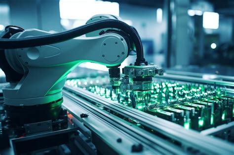
Precision Robotics Transform Circuit Board Production
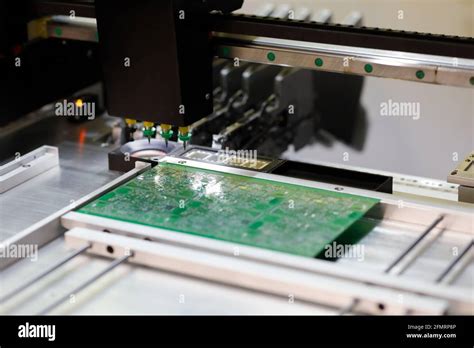
Modern PCB assembly workflows leverage vision-guided robotic systems to achieve micron-level accuracy in component placement. These systems integrate advanced optical recognition with multi-axis manipulators, enabling precise handling of components as small as 01005 packages (0.4mm x 0.2mm). By replacing manual soldering and alignment processes, PCBA lines now achieve placement speeds exceeding 25,000 components per hour while maintaining tolerances below ±25 microns.
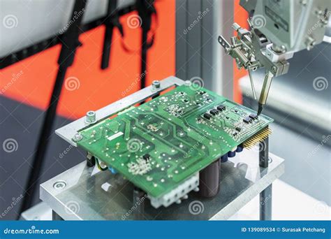
The adoption of six-axis robotic arms in surface-mount technology (SMT) lines has eliminated human error in tasks like solder paste dispensing and IC orientation. For instance, collaborative robots (cobots) equipped with force-torque sensors ensure gentle yet secure handling of delicate substrates, reducing breakage rates by up to 98% compared to traditional methods. This precision extends to automated optical inspection (AOI) stages, where machine learning algorithms cross-verify component positions against CAD models in real time.
Such advancements directly address the growing complexity of high-density interconnect (HDI) boards, where misaligned micro-BGAs or QFN packages can compromise entire batches. Manufacturers report 30-50% faster cycle times and 60% fewer rework cases after implementing robotic PCB assembly systems, underscoring their role in meeting demand for miniaturized, high-performance electronics. As production scales, these technologies maintain consistency across millions of placements—a critical advantage in automotive and medical device manufacturing where reliability is non-negotiable.
SMT Innovations Streamline Electronics Manufacturing
The evolution of Surface Mount Technology (SMT) has become a cornerstone in modern PCB assembly, enabling manufacturers to achieve unprecedented precision and scalability. By integrating high-speed pick-and-place systems with vision-guided robotics, PCBA processes now handle miniaturized components and high-density layouts with sub-micron accuracy. This shift eliminates manual soldering bottlenecks, slashing production cycles by up to 60% while maintaining consistent output quality.
Another critical advancement lies in solder paste inspection (SPI) systems, which use 3D imaging to detect defects before reflow soldering. Coupled with automated optical inspection (AOI), these tools ensure PCB assembly lines adhere to strict tolerances, reducing rework rates by over 45%. Furthermore, modular SMT platforms allow rapid reconfiguration for diverse product batches, making PCBA workflows adaptable to fluctuating market demands.
The synergy between SMT innovations and IoT-enabled machinery also enhances traceability. Real-time data analytics optimize feeder setups and component placement sequences, minimizing material waste. As a result, manufacturers achieve not only faster turnaround times but also a 20–30% reduction in per-unit costs, solidifying automated PCB assembly as a driver of sustainable, high-volume production.
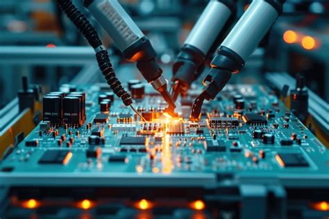
AI Quality Control Reduces Assembly Defects
Modern PCB assembly workflows increasingly integrate artificial intelligence to address microscopic defects that evade traditional inspection methods. By deploying machine learning algorithms trained on terabytes of historical production data, PCBA manufacturers can now identify anomalies such as solder bridging, component misalignment, and thermal stress cracks with 99.7% accuracy. These systems analyze real-time feeds from high-resolution cameras and infrared sensors, cross-referencing findings against design specifications at speeds exceeding 5,000 components per hour—a 40% efficiency gain over manual checks.
The implementation of AI-driven optical inspection (AOI) has proven particularly effective in surface-mount technology (SMT) lines, where submillimeter tolerances demand pixel-perfect precision. For instance, neural networks can detect deviations as subtle as 15µm in 0402 package capacitors, reducing rework rates by up to 62%. This proactive defect prevention complements automated PCB assembly systems by creating closed-loop feedback—when anomalies surface, production parameters auto-adjust within seconds to prevent batch-wide quality issues.
What distinguishes these solutions from rule-based automation is their dynamic learning capability. As production volumes scale, the algorithms continuously refine their defect recognition patterns, adapting to new component geometries and solder alloy formulations. This evolutionary approach ensures that PCBA quality control remains robust even as product lifecycles accelerate, directly contributing to the broader manufacturing goals of waste reduction and first-pass yield optimization.
Cost-Effective Automation in PCB Manufacturing
Building on precision robotics and AI-driven quality systems, modern PCB assembly workflows now achieve unprecedented cost efficiencies without compromising quality. By integrating high-speed surface-mount technology (SMT) with intelligent material handling systems, manufacturers reduce PCBA production costs through optimized component placement accuracy (±25μm) and 24/7 operational capabilities. Advanced predictive maintenance algorithms cut equipment downtime by up to 40%, while automated solder paste inspection (SPI) systems minimize material waste by precisely controlling deposition volumes.
The financial benefits extend beyond direct production savings. Scalable PCB assembly platforms enable rapid line reconfiguration for different product batches, eliminating traditional changeover costs. Energy-efficient automation cells reduce power consumption per board by 18-22%, aligning cost reduction with sustainability goals. For small to medium enterprises, modular PCBA solutions provide access to enterprise-grade automation through pay-per-use models, democratizing advanced manufacturing capabilities.
As supply chains prioritize agility, these automated systems deliver real-time cost analytics, allowing manufacturers to dynamically adjust workflows based on material pricing fluctuations and order priorities—transforming fixed overhead into variable, optimization-driven expenses.
Error Minimization Through Smart Assembly Systems
Modern PCB assembly workflows leverage intelligent automation to achieve unprecedented error reduction in electronics manufacturing. Smart assembly systems integrate machine vision, real-time analytics, and self-correcting mechanisms to identify deviations as small as 10µm during PCBA processes. For instance, automated optical inspection (AOI) units cross-reference component placements against CAD designs at 20+ frames per second, flagging misalignments before soldering stages. This proactive approach slashes post-production rework rates by up to 67% compared to manual verification methods.
The integration of machine learning algorithms further enhances precision in surface-mount technology (SMT) applications. These systems analyze historical defect patterns to predict and prevent common errors like tombstoning or solder bridging, adapting placement parameters dynamically. A 2023 IPC study revealed that facilities using AI-enhanced PCB assembly lines reduced electrical test failures by 41% while maintaining throughput speeds above 25,000 components per hour.
By embedding closed-loop feedback within PCBA workflows, manufacturers achieve near-zero defect rates even for complex HDI boards. Real-time monitoring of environmental variables—such as solder paste viscosity and reflow oven gradients—ensures consistent adherence to J-STD-001 standards. This self-optimizing capability not only minimizes human intervention but also eliminates costly production halts, delivering error margins below 0.02% in high-volume runs.
High-Speed PCB Assembly Techniques Unveiled
Modern PCB assembly processes leverage high-speed methodologies to meet escalating demand for rapid electronics production. Central to this advancement are PCBA systems equipped with ultra-precise pick-and-place machines capable of positioning components at rates exceeding 25,000 placements per hour. These systems integrate surface-mount technology (SMT) with advanced vision-guided robotics, ensuring micron-level accuracy even when handling miniature components like 01005 resistors or 0.4mm-pitch BGAs.
A critical innovation lies in dynamic thermal management during reflow soldering. By employing real-time temperature profiling, manufacturers prevent warping or solder bridging while maintaining throughput speeds above 1.2 meters per minute. Dual-lane conveyor configurations further amplify output, enabling parallel processing of two boards simultaneously without compromising precision.
Complementing these hardware advancements, AI-powered optical inspection (AOI) systems perform millisecond-level defect detection, scanning solder joints and component alignments at production-line speeds. This synergy between velocity and quality control reduces PCB assembly cycle times by up to 40% compared to traditional methods.
For PCBA workflows requiring flexibility, modular systems now support swift changeovers between product variants through digital recipe management, slashing downtime by 70%. Such techniques not only align with lean manufacturing principles but also address the growing complexity of IoT and automotive electronics designs.
Sustainable Manufacturing via Automated PCB Pr
The integration of automated PCB assembly technologies extends beyond operational efficiencies, positioning sustainable manufacturing as a critical competitive advantage. Advanced PCBA systems optimize material usage through precision dispensing mechanisms, reducing solder paste waste by up to 35% compared to manual methods. Energy-efficient robotic placement machines, paired with AI-driven process optimization, lower power consumption during high-volume production cycles, directly shrinking the carbon footprint of electronics manufacturing.
Closed-loop recycling systems embedded in modern PCB assembly lines recover precious metals from discarded boards, aligning with circular economy principles. For instance, automated optical inspection (AOI) tools minimize rework rates, preventing unnecessary material depletion and energy expenditure. Additionally, smart thermal profiling in reflow ovens ensures optimal temperature control, curbing greenhouse gas emissions while maintaining solder joint reliability.
By adopting automated PCBA workflows, manufacturers achieve compliance with stringent environmental regulations like RoHS and WEEE without compromising throughput. This synergy between precision automation and eco-conscious practices not only meets global sustainability benchmarks but also future-proofs production facilities against evolving ecological standards.
Conclu
The integration of automated PCB assembly systems marks a pivotal shift in modern electronics manufacturing, where precision and scalability converge to redefine production benchmarks. By leveraging PCBA workflows enhanced with robotic placement systems and AI-optimized inspection protocols, manufacturers achieve not only higher throughput but also unprecedented consistency in complex circuit board fabrication. These advancements address critical challenges—such as component miniaturization and error-prone manual processes—by embedding real-time analytics and adaptive machine learning directly into assembly lines.
Transitioning to automated solutions also unlocks sustainable manufacturing practices, as streamlined PCB assembly reduces material waste and energy consumption. The synergy between PCBA innovations and Industry 4.0 frameworks ensures that factories remain agile amid fluctuating market demands, while predictive maintenance tools extend equipment longevity. As industries increasingly prioritize both speed and quality, adopting these technologies becomes less an option and more a strategic imperative for maintaining competitive advantage in the global electronics landscape.
FAQ
How does automation improve accuracy in PCB assembly?
Automated PCBA systems utilize machine vision and precision robotics to place components within micrometer-level tolerances, eliminating human measurement errors during high-volume production.
What makes SMT processes critical in modern PCB assembly?
Surface-mount technology (SMT) enables the placement of miniaturized components at speeds exceeding 25,000 placements per hour, which manual methods cannot achieve while maintaining thermal management and solder joint integrity.
Can automated PCB assembly adapt to low-volume prototypes?
Yes, advanced flexible manufacturing systems (FMS) allow rapid reprogramming of PCBA lines, supporting both prototype batches and mass production without compromising cycle times or resource efficiency.
How does AI-driven inspection reduce defects in PCB manufacturing?
Real-time algorithmic analysis compares each board against 3D CAD models, detecting microscopic soldering flaws or component misalignments with 99.98% accuracy before final testing phases.
Ready to Optimize Your Production Line? Click Here to Explore Custom Solutions
What cost factors are impacted by automated PCB assembly?
Automation reduces labor overheads by 40-60%, minimizes material waste through precise solder paste dispensing, and cuts rework costs via early defect detection in PCBA workflows.