Automated PCB Manufacturing: Revolutionizing the Electronics Industry
Introduction
The electronics industry has undergone a transformative evolution over the past few decades, driven by advancements in technology and the increasing demand for smaller, faster, and more efficient electronic devices. At the heart of this evolution lies the Printed Circuit Board (PCB), which serves as the foundation for virtually all electronic devices. As the complexity of electronic devices has grown, so too has the need for more sophisticated and efficient methods of PCB manufacturing. Enter automated PCB manufacturing—a process that leverages cutting-edge technology to streamline production, improve precision, and reduce costs. This article delves into the world of automated PCB manufacturing, exploring its key components, benefits, challenges, and future prospects.
The Evolution of PCB Manufacturing
To appreciate the significance of automated PCB manufacturing, it is essential to understand the evolution of PCB production. Traditional PCB manufacturing was a labor-intensive process that involved multiple manual steps, including designing, etching, drilling, and soldering. These processes were not only time-consuming but also prone to human error, leading to defects and inconsistencies in the final product.
As the demand for electronic devices surged, manufacturers sought ways to increase production efficiency and improve the quality of PCBs. The advent of Computer-Aided Design (CAD) and Computer-Aided Manufacturing (CAM) marked the beginning of a new era in PCB production. These technologies enabled designers to create intricate PCB layouts with greater precision, while automated machinery began to take over many of the manual tasks involved in manufacturing.
Today, automated PCB manufacturing represents the pinnacle of this evolution, integrating advanced technologies such as robotics, artificial intelligence (AI), and the Internet of Things (IoT) to create a seamless, highly efficient production process.
Key Components of Automated PCB Manufacturing
Automated PCB manufacturing encompasses a wide range of processes, each of which plays a critical role in ensuring the quality and reliability of the final product. The following are some of the key components of automated PCB manufacturing:
- Design and Prototyping:
The first step in automated PCB manufacturing is the design phase, where engineers use CAD software to create a detailed blueprint of the PCB. This design is then converted into a digital format that can be interpreted by automated machinery. Prototyping is an essential part of this process, allowing manufacturers to test and refine the design before moving on to full-scale production. - Material Preparation:
Once the design is finalized, the next step is to prepare the materials that will be used to create the PCB. This typically involves cutting the substrate material (usually a type of fiberglass) to the required size and applying a layer of copper to form the conductive pathways. Automated machinery is used to ensure that these materials are prepared with precision and consistency. - Printing and Etching:
The PCB design is then printed onto the substrate using a process known as photolithography. This involves applying a light-sensitive chemical (photoresist) to the copper layer and then exposing it to ultraviolet light through a mask that contains the PCB design. The exposed areas of the photoresist harden, while the unexposed areas remain soft and can be washed away. The remaining photoresist acts as a protective layer, allowing the underlying copper to be etched away, leaving behind the desired circuit pattern. - Drilling and Plating:
After the circuit pattern has been etched, the next step is to drill holes into the PCB to accommodate components and vias (electrical connections between layers). Automated drilling machines are used to ensure that the holes are drilled with pinpoint accuracy. Once the holes are drilled, they are plated with a conductive material (usually copper) to establish electrical connections between the layers of the PCB. - Solder Mask Application:
A solder mask is then applied to the PCB to protect the copper traces from oxidation and to prevent solder bridges from forming during the assembly process. The solder mask is typically applied using a screen-printing process, and automated machinery ensures that it is applied evenly and accurately. - Surface Finish:
The final step in the PCB manufacturing process is the application of a surface finish, which protects the exposed copper and ensures that the PCB is ready for component assembly. Common surface finishes include Hot Air Solder Leveling (HASL), Electroless Nickel Immersion Gold (ENIG), and Organic Solderability Preservative (OSP). Automated machinery is used to apply these finishes with precision and consistency. - Component Assembly:
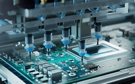
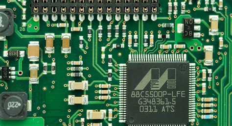
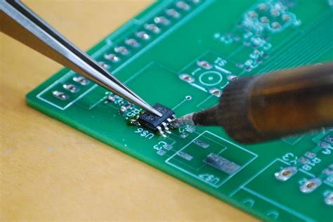
Once the PCB is complete, the next step is to assemble the electronic components onto the board. This process, known as Surface Mount Technology (SMT), involves placing components onto the PCB and then soldering them in place using a reflow oven. Automated pick-and-place machines are used to ensure that components are placed with high precision, while automated optical inspection (AOI) systems are used to verify the quality of the assembly. - Testing and Quality Control:
The final step in the automated PCB manufacturing process is testing and quality control. Automated testing equipment is used to verify that the PCB functions as intended and that there are no defects or faults. This may include electrical testing, functional testing, and environmental testing to ensure that the PCB can withstand the conditions it will be exposed to in its final application.
Benefits of Automated PCB Manufacturing
The adoption of automated PCB manufacturing offers a wide range of benefits to manufacturers, including:
- Increased Efficiency:
One of the most significant advantages of automated PCB manufacturing is the increase in production efficiency. Automated machinery can perform tasks much faster than human workers, leading to shorter production cycles and higher output rates. This allows manufacturers to meet the growing demand for electronic devices without compromising on quality. - Improved Precision and Consistency:
Automated machinery is capable of performing tasks with a level of precision and consistency that is difficult to achieve with manual labor. This results in fewer defects and higher-quality PCBs, which in turn leads to more reliable electronic devices. - Reduced Labor Costs:
By automating many of the tasks involved in PCB manufacturing, companies can significantly reduce their labor costs. This is particularly important in regions where labor costs are high, as it allows manufacturers to remain competitive in the global market. - Enhanced Flexibility:
Automated PCB manufacturing systems are highly flexible and can be easily reconfigured to accommodate different PCB designs and production requirements. This allows manufacturers to quickly adapt to changes in demand or to produce custom PCBs for specific applications. - Improved Safety:
Many of the tasks involved in traditional PCB manufacturing, such as etching and soldering, involve the use of hazardous chemicals and high temperatures. By automating these processes, manufacturers can reduce the risk of workplace accidents and create a safer working environment for their employees. - Scalability:
Automated PCB manufacturing systems are highly scalable, allowing manufacturers to easily increase production capacity as demand grows. This is particularly important for companies that are looking to expand their operations or enter new markets.
Challenges of Automated PCB Manufacturing
While automated PCB manufacturing offers numerous benefits, it is not without its challenges. Some of the key challenges include:
- High Initial Investment:
The initial cost of setting up an automated PCB manufacturing facility can be prohibitively high, particularly for small and medium-sized enterprises (SMEs). The cost of purchasing and installing automated machinery, as well as the cost of training employees to operate and maintain the equipment, can be a significant barrier to entry. - Complexity:
Automated PCB manufacturing systems are highly complex and require a high level of expertise to design, implement, and maintain. This can be a challenge for companies that do not have the necessary technical knowledge or resources. - Maintenance and Downtime:
Automated machinery requires regular maintenance to ensure that it continues to operate efficiently. Any downtime due to equipment failure or maintenance can result in significant production delays and lost revenue. - Integration with Existing Systems:
Integrating automated PCB manufacturing systems with existing production processes can be a complex and time-consuming task. This is particularly true for companies that are transitioning from traditional manufacturing methods to automated systems. - Quality Control:
While automated systems are capable of producing high-quality PCBs, they are not infallible. Ensuring that the final product meets the required quality standards still requires rigorous testing and quality control processes.
Future Prospects of Automated PCB Manufacturing
The future of automated PCB manufacturing looks promising, with several emerging trends and technologies poised to further revolutionize the industry. Some of the key trends to watch include:
- Artificial Intelligence (AI) and Machine Learning:
AI and machine learning are increasingly being integrated into automated PCB manufacturing systems to optimize production processes and improve quality control. These technologies can analyze vast amounts of data in real-time, allowing manufacturers to identify and address potential issues before they become problems. - Internet of Things (IoT):
The IoT is playing an increasingly important role in automated PCB manufacturing, enabling machines to communicate with each other and with central control systems. This allows for greater coordination and efficiency in the production process, as well as real-time monitoring and diagnostics. - Additive Manufacturing (3D Printing):
Additive manufacturing, or 3D printing, is emerging as a potential game-changer in PCB manufacturing. This technology allows for the creation of complex, multi-layered PCBs with greater precision and flexibility than traditional methods. While still in its early stages, 3D printing has the potential to significantly reduce production times and costs. - Advanced Materials:
The development of new materials, such as flexible and stretchable substrates, is opening up new possibilities for PCB design and manufacturing. These materials allow for the creation of PCBs that can be bent, folded, or stretched, making them ideal for use in wearable devices and other innovative applications. - Sustainability:
As environmental concerns continue to grow, there is increasing pressure on manufacturers to adopt more sustainable practices. Automated PCB manufacturing systems are being designed with sustainability in mind, incorporating energy-efficient technologies and reducing waste through more precise material usage.
Conclusion
Automated PCB manufacturing represents a significant leap forward in the production of electronic devices, offering numerous benefits in terms of efficiency, precision, and cost-effectiveness. While there are challenges to overcome, the continued advancement of technology is likely to drive further innovation in this field, paving the way for even more sophisticated and efficient manufacturing processes. As the demand for electronic devices continues to grow, automated PCB manufacturing will play an increasingly important role in meeting this demand and shaping the future of the electronics industry.