Advanced EMS PCB Assembly Techniques for Modern Electronics

Key Takeaways
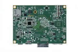
Modern PCB assembly processes rely on precision techniques to meet the demands of high-performance electronics. PCBA (Printed Circuit Board Assembly) now integrates advanced methods such as laser-assisted soldering and microscopic component placement, ensuring minimal error margins in densely packed designs. Automated systems play a pivotal role, with automated optical inspection (AOI) detecting defects as small as 10µm, significantly reducing post-production failures.
"The shift toward automation in EMS PCB assembly isn’t just about speed—it’s about achieving repeatable accuracy in complex designs," notes a leading industry engineer.
A critical focus area is thermal management, where materials like high-conductivity substrates and embedded heat sinks mitigate overheating risks in power-intensive devices. Below is a comparison of traditional vs. advanced thermal solutions:
| Technique | Traditional Approach | Advanced Solution |
|---|---|---|
| Heat Dissipation | Aluminum heat sinks | Graphene-enhanced layers |
| Substrate Material | FR-4 | Ceramic-filled polymers |
| Component Layout | Manual optimization | AI-driven thermal simulation |
For reliability optimization, manufacturers prioritize conformal coating and vibration-resistant soldering to withstand harsh operating environments.
Tip: Always validate solder joint integrity using 3D X-ray inspection during PCBA to catch hidden flaws.
By combining robust EMS techniques with data-driven process controls, modern electronics achieve longer lifespans and consistent performance—key factors in industries like aerospace and medical devices.

Precision Soldering in EMS PCB Assembly
In modern PCB assembly, precision soldering forms the backbone of creating reliable electronic devices. Advanced PCBA processes leverage techniques like reflow soldering and solder paste stenciling to ensure micron-level accuracy, particularly for high-density components. Automated systems now integrate laser-guided placement and nitrogen-reflow environments to minimize oxidation, enhancing joint integrity even in complex, multi-layer boards.
The shift toward miniaturized electronics demands tighter control over thermal profiles during soldering. EMS providers employ real-time monitoring tools to adjust heat distribution, preventing issues like tombstoning or cold joints. For mixed-technology boards, selective soldering combines wave and hand-soldering methods to accommodate both surface-mount (SMT) and through-hole components seamlessly.
Material selection also plays a critical role. High-grade solder alloys with low silver content improve wettability, while no-clean fluxes reduce post-process residue. This meticulous approach not only aligns with industry standards like IPC-A-610 but also ensures compatibility with subsequent automated optical inspection stages. By balancing speed and precision, PCBA specialists achieve repeatable results, laying the foundation for robust thermal management and long-term device reliability.
Automated Inspection for Electronics Quality
In PCB assembly, ensuring consistent quality demands rigorous inspection protocols. Modern EMS providers leverage automated optical inspection (AOI) systems to detect microscopic defects—such as misaligned components, solder bridges, or insufficient joints—with unparalleled accuracy. These systems utilize high-resolution cameras and machine learning algorithms to compare PCBA units against predefined design specifications, flagging discrepancies in real time. By integrating statistical process control (SPC), manufacturers can identify trends in production errors, enabling proactive adjustments to soldering parameters or component placement workflows.
Complementing AOI, advanced X-ray inspection techniques scrutinize hidden connections in multilayer boards or ball grid array (BGA) packages, ensuring integrity in complex PCB assembly designs. For high-volume production, in-circuit testing (ICT) validates electrical functionality, verifying resistance, capacitance, and signal continuity across circuits. This multilayered approach minimizes human error while accelerating throughput, critical for meeting stringent industry standards.
By embedding these automated processes into PCBA workflows, EMS partners achieve near-zero defect rates, directly enhancing end-product reliability. Such precision not only reduces rework costs but also strengthens compliance with automotive, medical, and aerospace quality benchmarks—a cornerstone for next-generation electronics manufacturing.

Thermal Management in PCB Manufacturing
Effective thermal management is critical in modern PCB assembly processes, particularly as electronic devices demand higher power densities and miniaturized designs. Managing heat dissipation ensures long-term reliability and prevents performance degradation in components like processors, power modules, and RF circuits. Advanced PCBA techniques employ thermally conductive substrates, such as metal-core or ceramic-based materials, to enhance heat transfer away from sensitive areas. Additionally, copper-filled vias and strategically placed heat sinks optimize thermal pathways, reducing hotspots across the board.
Automated design tools now integrate thermal simulation software, enabling engineers to predict and address heat distribution challenges during the layout phase. This proactive approach minimizes rework in PCB assembly by identifying potential issues before production. For high-frequency or high-power applications, thermal interface materials (TIMs) like silicone pads or epoxy adhesives further improve conductivity between components and cooling systems.
In PCBA workflows, balancing thermal performance with mechanical constraints requires precise component placement and material selection. For instance, low-thermal-resistance solders and optimized trace widths help maintain stability under thermal stress. By combining these strategies, manufacturers achieve robust thermal management that aligns with the demands of next-generation electronics, ensuring devices operate efficiently even in extreme environments.
High-Performance Device Assembly Methods
Achieving optimal performance in modern electronics demands meticulous PCB assembly processes tailored for high-density, high-speed applications. Advanced PCBA workflows now integrate surface-mount technology (SMT) with precision robotics to place miniature components at speeds exceeding 50,000 placements per hour, ensuring micron-level accuracy. Thermally conductive underfills and laser-assisted reflow soldering further enhance structural integrity, critical for devices operating in extreme environments.
Central to these processes is the synchronization of PCB assembly stages with real-time quality analytics. Automated systems monitor solder joint formation, detecting voids or misalignments early to minimize rework. For high-frequency circuits, impedance-controlled stacking and signal integrity validation ensure minimal electromagnetic interference (EMI). Additionally, PCBA workflows employ conformal coating techniques to shield sensitive components from moisture and contaminants, extending product lifespans.
Transitioning to next-gen assembly, manufacturers prioritize design-for-manufacturability (DFM) checks to preempt thermal stress and mechanical fatigue. By aligning material selection with operational demands—such as high-Tg laminates for elevated temperatures—PCB assembly achieves reliability without compromising miniaturization trends. These methods not only support IoT and 5G devices but also lay the groundwork for scalable, high-yield production in evolving tech landscapes.

Robust EMS Techniques for Modern Electronics
Modern electronics demand PCB assembly processes that prioritize durability and precision, particularly as devices grow smaller and more complex. To address these challenges, advanced EMS providers employ robust techniques such as high-precision solder paste stenciling and conformal coating to ensure long-term reliability. These methods mitigate risks like solder joint fatigue or moisture ingress, which are critical in harsh operating environments.
Integrating automated optical inspection (AOI) systems further strengthens quality control by detecting microscopic defects in PCBA layouts, such as misaligned components or insufficient solder coverage. This level of scrutiny is essential for applications in automotive or industrial electronics, where failure rates must remain near zero. Additionally, thermal profiling during reflow soldering ensures uniform heat distribution, preventing warping or delamination in multi-layer boards.
By combining these strategies with materials engineered for thermal stability—such as high-Tg substrates—EMS specialists achieve a balance between miniaturization and resilience. This approach not only aligns with the demands of next-gen IoT and wearable tech but also reinforces the lifecycle performance of mission-critical systems.

Optimizing PCB Reliability With Advanced EMS
Achieving long-term reliability in PCB assembly requires integrating advanced EMS strategies that address both design and manufacturing challenges. A cornerstone of this approach is the application of precision-controlled soldering processes, which minimize voids and cold joints—common failure points in PCBA. By leveraging techniques such as nitrogen-reflow soldering, manufacturers reduce oxidation risks while ensuring consistent electrical connectivity across high-density interconnects.
Another critical factor is the implementation of automated optical inspection (AOI) systems, which detect microscopic defects like solder bridging or component misalignment. These systems analyze PCB assembly outputs in real time, enabling rapid corrections before defects escalate into field failures. Combined with thermal profiling tools, AOI ensures components operate within safe temperature thresholds, extending device lifespans.
Advanced EMS providers also prioritize thermal management solutions during PCBA design, incorporating materials like metal-core substrates or thermally conductive adhesives. This mitigates thermal stress on sensitive components, particularly in applications such as automotive or industrial electronics. Additionally, accelerated life testing (ALT) simulates years of operational stress in controlled environments, validating design choices and refining assembly protocols.
By harmonizing these techniques, modern EMS workflows deliver PCB assembly outcomes that meet stringent reliability standards, ensuring devices perform consistently even under extreme conditions.
Next-Gen Soldering Solutions for PCBs
Modern PCB assembly processes demand soldering techniques that balance precision, scalability, and sustainability. Innovations like lead-free solder alloys and laser-assisted reflow are redefining reliability in PCBA, particularly for high-density designs with micro-BGA components or ultra-fine pitch ICs. Advanced systems now integrate adaptive thermal profiling, dynamically adjusting heat distribution across the board to prevent warping or solder joint fractures. This is critical for applications requiring thermal cycling resistance, such as automotive or aerospace electronics.
Automated soldering platforms, equipped with AI-driven vision systems, ensure micron-level accuracy while minimizing human error. These systems analyze solder paste deposition in real-time, correcting deviations before reflow—a key factor in reducing post-assembly defects. Additionally, low-voiding solder pastes enhance electrical conductivity and mechanical stability, especially in high-frequency or power-intensive devices.
The shift toward environmentally conscious manufacturing has also spurred adoption of halogen-free fluxes and recyclable solder materials, aligning PCB assembly with global sustainability standards. By combining these advancements, manufacturers achieve faster cycle times, higher yield rates, and improved longevity for mission-critical electronics. This progression seamlessly supports subsequent stages like automated optical inspection, ensuring end-to-end quality in modern PCBA workflows.

Automated Optical Inspection Best Practices
In modern PCB assembly workflows, automated optical inspection (AOI) has become indispensable for ensuring zero-defect manufacturing standards. By leveraging high-resolution cameras and advanced algorithms, AOI systems detect microscopic flaws—such as solder bridges, missing components, or misaligned traces—that manual inspections might overlook. For PCBA processes, optimizing AOI begins with calibration protocols: aligning lighting angles to eliminate glare and configuring threshold parameters to balance sensitivity with false-positive rates.
A critical best practice involves integrating AOI at multiple stages—post-solder paste application, post-reflow, and post-final assembly—to intercept defects early. For instance, pre-reflow inspections identify paste deposition irregularities, preventing downstream rework costs. Advanced systems now employ 3D imaging and machine learning to adapt to complex board geometries, particularly in high-density PCB assembly projects.
To maximize ROI, EMS providers pair AOI with statistical process control (SPC) tools, correlating defect patterns with process variables like solder paste viscosity or oven temperature profiles. This data-driven approach not only enhances PCBA reliability but also strengthens thermal management outcomes by flagging insufficient solder joints that could compromise heat dissipation. By refining these strategies, manufacturers achieve tighter tolerances while maintaining alignment with industry benchmarks like IPC-A-610.
Conclusion
The evolution of PCB assembly methodologies underscores the critical role of integrating precision, automation, and innovation in modern electronics manufacturing. As the industry shifts toward miniaturization and higher complexity, advanced PCBA techniques—such as laser-assisted soldering and AI-driven defect detection—have become indispensable for ensuring device reliability. These processes not only address challenges in thermal dissipation and component density but also enable scalable production without compromising quality.
Transitioning from traditional methods, contemporary PCB assembly workflows now leverage real-time monitoring systems and adaptive thermal management protocols, which mitigate risks like delamination or solder joint fatigue. Furthermore, the adoption of environmentally resistant materials in PCBA aligns with global demands for durable, high-performance electronics across industries such as automotive and IoT. By prioritizing both precision and adaptability, manufacturers can navigate the delicate balance between accelerating time-to-market and maintaining rigorous performance benchmarks.
Ultimately, the convergence of these strategies establishes a foundation for next-generation electronics, where PCB assembly excellence directly correlates with product longevity and user trust. As innovation continues to reshape the landscape, embracing these advanced techniques will remain pivotal for sustaining competitiveness in an increasingly dynamic technological ecosystem.
Frequently Asked Questions
What distinguishes PCB assembly from PCBA?
PCB assembly refers to the process of populating a bare circuit board with components, while PCBA (Printed Circuit Board Assembly) denotes the fully assembled and functional board. Modern EMS PCB assembly services integrate both stages, ensuring seamless transitions from component placement to final testing.
How does automated inspection improve PCB reliability?
Advanced automated optical inspection (AOI) systems detect micro-defects like solder bridges or misaligned components, reducing human error. Coupled with X-ray inspection for hidden joints, these techniques align with high-performance device assembly standards, ensuring consistent quality.
Why is thermal management critical in electronics manufacturing?
Effective thermal management prevents overheating in densely packed PCBA designs, extending device lifespan. Techniques like thermal vias and heat-dissipating materials are integrated during EMS PCB assembly to maintain optimal operating temperatures.
Can precision soldering techniques be applied to miniaturized components?
Yes, laser soldering and micro-soldering methods enable accurate connections for components as small as 01005 packages. These processes are vital for modern electronics, supporting compact, high-density PCB assembly without compromising durability.
Explore Advanced PCB Assembly Solutions
For tailored EMS PCB assembly services that prioritize precision and reliability, please click here to discover how our expertise can elevate your electronics manufacturing projects.
