Streamlining PCB Assembly for Efficient Electronics Production
Key Takeaways
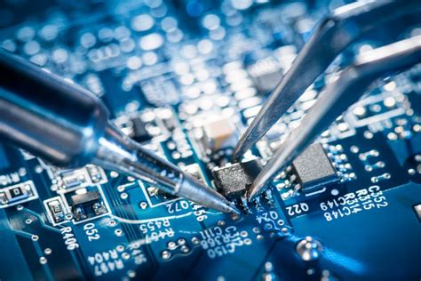
Effective PCB assembly requires balancing speed, accuracy, and cost-efficiency. By adopting automated pick-and-place systems and design for manufacturability (DFM) principles, manufacturers can reduce PCBA cycle times while maintaining component alignment tolerances of ±0.05mm.
"Optimizing solder paste application and reflow profiling remains critical—improper thermal management accounts for 34% of post-assembly defects."
| Technique | Traditional Approach | Optimized Method |
|---|---|---|
| Component Placement | Manual alignment | Vision-guided robotics |
| Testing | End-of-line checks | In-line AOI systems |
| Material Utilization | 82% efficiency | 95% efficiency |
Integrating PCB assembly workflows with enterprise resource planning (ERP) software enables real-time inventory tracking, reducing material shortages by up to 40%. For PCBA projects requiring mixed-technology boards, combining surface-mount technology (SMT) with selective soldering minimizes thermal stress on sensitive components like BGAs.
To enhance reproducibility, standardized process documentation should accompany every PCB assembly order, detailing solder mask requirements and IPC-A-610 Class 2/3 compliance parameters. This practice reduces rework rates by 28% in high-volume production environments.
Optimizing PCB Assembly for Faster Production
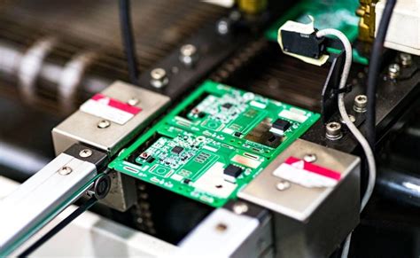
Modern PCB assembly workflows require strategic adjustments to accelerate production without compromising reliability. Implementing automated pick-and-place systems can reduce manual handling errors while increasing placement speeds by up to 40%, particularly in high-volume PCBA runs. Designers should prioritize panelization strategies to maximize board space utilization, allowing multiple units to be processed simultaneously during soldering and inspection phases.
Integrating design-for-manufacturing (DFM) principles early in the development cycle minimizes post-production revisions, ensuring smoother transitions from prototyping to full-scale PCB assembly. For instance, standardizing component footprints and avoiding ultra-fine pitch layouts can prevent machine recalibration delays. Real-time monitoring systems further enhance throughput by identifying bottlenecks in solder paste application or reflow oven workflows.
Material selection also plays a critical role—opting for lead-free solder alloys with optimized melting profiles shortens thermal cycling times. Pairing these technical upgrades with synchronized logistics, such as just-in-time component delivery, creates a cohesive acceleration framework. By aligning PCBA processes with lean manufacturing methodologies, manufacturers can achieve 25–30% faster cycle times while maintaining the precision required for complex electronics. This approach naturally dovetails with cost-reduction strategies, setting the stage for scalable, high-efficiency production models.
Cost-Effective PCB Assembly Techniques
Achieving cost efficiency in PCB assembly requires balancing precision with strategic resource allocation. One proven method involves optimizing design for manufacturability (DFM) principles, which minimize material waste and reduce rework by aligning layouts with production capabilities. For instance, standardizing component sizes and footprints across designs lowers procurement costs and simplifies PCBA workflows.
Leveraging automated assembly lines with pick-and-place systems accelerates throughput while maintaining consistency, particularly for high-volume orders. Bulk purchasing of commonly used components, such as resistors and capacitors, further drives down per-unit expenses. However, cost savings should never compromise quality—implementing automated optical inspection (AOI) at critical stages ensures defects are identified early, avoiding costly post-production corrections.
Another approach involves partnering with suppliers offering consolidated services, such as combined PCB assembly and testing, to reduce logistical overhead. Modular design strategies also enable reuse of validated circuit blocks across multiple projects, trimming development time and material costs. By integrating these techniques, manufacturers can streamline PCBA processes while adhering to tight budgets, creating a foundation for scalable electronics production.
Precision Component Integration Strategies
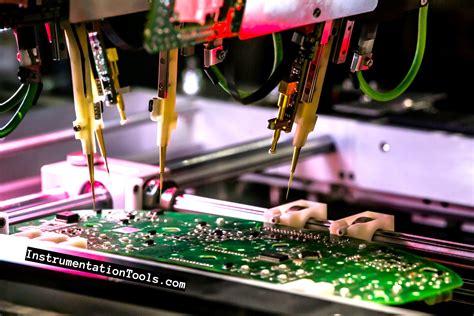
Achieving precision in PCB assembly requires meticulous planning at every stage of component integration. Modern PCBA workflows leverage automated pick-and-place systems to ensure micron-level accuracy when positioning surface-mount devices (SMDs) or through-hole components. Advanced vision alignment systems calibrate placement parameters in real time, minimizing deviations caused by thermal expansion or mechanical drift. For high-density designs, laser-assisted soldering enables precise bonding of fine-pitch components, such as 01005 packages, without compromising adjacent circuits.
Integrating mixed-technology boards—combining SMDs, BGAs, and through-hole parts—demands strategic sequencing. For instance, placing heat-sensitive components after reflow processes reduces thermal stress, while selective soldering optimizes joint integrity for larger connectors. To maintain consistency, manufacturers often adopt closed-loop feedback systems that correlate placement data with post-assembly inspections, refining machine learning algorithms for future runs.
Alignment with Design for Manufacturing (DFM) principles further streamlines integration. By optimizing pad geometries, solder mask apertures, and component spacing during the design phase, PCB assembly teams reduce rework rates and enhance yield. Real-time monitoring of stencil printing and reflow profiles ensures uniform solder paste deposition and reliable intermetallic bonding. Such strategies not only accelerate PCBA timelines but also align with broader goals of cost reduction and quality assurance in electronics production.
Enhancing Quality Control in PCB Assembly
Effective quality assurance in PCB assembly hinges on systematic inspection protocols and advanced testing methodologies. Modern PCBA workflows integrate automated optical inspection (AOI) and X-ray testing to identify defects like solder bridging, misaligned components, or voids in ball grid arrays. These technologies enable real-time defect detection, reducing post-production rework by up to 40% while ensuring compliance with IPC-A-610 standards.
To maintain precision, manufacturers employ statistical process control (SPC) tools to monitor critical parameters such as solder paste deposition thickness and reflow oven temperature profiles. Pairing these with in-circuit testing (ICT) and functional testing validates electrical performance, ensuring each assembled board meets design specifications. For high-reliability applications, environmental stress screening (ESS) simulates operational conditions to weed out latent failures.
Collaboration between PCB assembly teams and component suppliers further strengthens quality outcomes. Implementing traceability systems with barcoded materials ensures accountability across the supply chain, while first-article inspection (FAI) protocols verify initial production batches against golden samples. By embedding these practices into PCBA workflows, manufacturers achieve near-zero defect rates without compromising throughput—a critical balance for cost-sensitive electronics production.
Streamlined Electronics Manufacturing Processes
Modern PCB assembly relies on streamlined processes to eliminate bottlenecks and accelerate production cycles. By implementing automated PCBA workflows, manufacturers reduce manual intervention while maintaining precision in component placement and soldering. For example, standardized design-for-manufacturing (DFM) protocols ensure compatibility between circuit layouts and assembly equipment, minimizing rework and material waste.
A critical aspect of optimization lies in synchronizing PCB assembly stages with upstream design and downstream testing. This integration allows real-time adjustments using data analytics, ensuring rapid identification of process inefficiencies. Advanced surface-mount technology (SMT) lines, combined with modular conveyor systems, enable flexible scaling for high-mix, low-volume production runs without sacrificing speed.
Moreover, lean manufacturing principles—such as just-in-time inventory management—reduce component staging delays. Collaborative robotics (cobots) further enhance throughput by handling repetitive tasks like board handling or solder paste application, freeing technicians for quality assurance roles.
To sustain efficiency, manufacturers adopt unified software platforms that track PCBA metrics—from solder joint integrity to thermal performance—across all production phases. This approach not only streamlines workflows but also aligns with evolving industry standards for energy-efficient and cost-effective electronics manufacturing. By balancing automation with human expertise, companies achieve faster time-to-market while maintaining rigorous quality benchmarks.
Boosting Efficiency in PCB Assembly Lines
Modern PCB assembly workflows demand strategic optimization to meet rising production targets without compromising quality. A primary driver of efficiency lies in automating repetitive tasks, such as solder paste application and component placement, which reduces human error and accelerates throughput. Advanced PCBA lines now integrate IoT-enabled sensors to monitor equipment performance in real time, enabling predictive maintenance that minimizes unplanned downtime.
Another critical factor involves standardizing design-for-manufacturing (DFM) guidelines across teams. By aligning circuit board layouts with PCB assembly capabilities early in the design phase, manufacturers can avoid costly rework and streamline material procurement. For instance, unified component libraries ensure consistent part availability, reducing delays caused by last-minute substitutions.
Modular production setups further enhance flexibility, allowing PCBA lines to swiftly adapt to varying batch sizes or product iterations. Pairing this with data-driven analytics helps identify bottlenecks—like solder reflow cycle times or inspection lag—enabling targeted process adjustments. Implementing automated optical inspection (AOI) systems at multiple checkpoints ensures defects are caught early, preventing downstream quality issues.
Ultimately, balancing speed with precision requires a harmonized approach where equipment upgrades, workforce training, and intelligent software tools operate synergistically. This not only elevates output rates but also strengthens the foundation for scalable electronics manufacturing.
Reducing Costs in Electronics Production
Achieving cost efficiency in PCB assembly requires a strategic balance between material selection, process optimization, and supply chain management. By leveraging standardized components in PCBA designs, manufacturers can minimize procurement delays and reduce inventory overhead. For instance, adopting panelization techniques—grouping multiple boards into a single panel—optimizes material usage and accelerates throughput during solder paste application and component placement.
Automation plays a pivotal role in trimming labor expenses while maintaining consistency. Robotic pick-and-place systems, integrated with machine vision, ensure precise component alignment, reducing rework rates and material waste. Additionally, implementing design-for-manufacturing (DFM) principles early in the PCB assembly workflow prevents costly revisions by aligning layouts with production capabilities.
Collaborating with suppliers for bulk purchasing of high-demand ICs or passive components further lowers per-unit costs. Meanwhile, modular testing protocols—such as in-circuit testing (ICT) at key PCBA stages—identify defects early, avoiding downstream quality failures. By combining these approaches, manufacturers can achieve at least 15–20% savings without compromising the reliability or precision of the final product.
Maintaining Precision in PCB Manufacturing
Achieving consistent precision in PCB assembly requires a meticulous balance of advanced technologies and rigorous process controls. Modern high-density interconnect (HDI) designs demand PCBA workflows capable of handling components with sub-millimeter accuracy, particularly for applications like IoT devices or medical electronics. Automated optical inspection (AOI) systems and laser-aligned pick-and-place machines ensure micron-level placement accuracy, reducing human error during component integration.
To maintain alignment with PCB assembly tolerances, manufacturers employ real-time thermal profiling during reflow soldering, preventing warping or solder bridging in temperature-sensitive materials. Traceability systems further enhance precision by tracking lot-specific material properties and process parameters across production batches. For PCBA involving mixed-technology boards, dual-purpose solder paste formulations enable seamless integration of surface-mount and through-hole components without compromising joint integrity.
Precision extends beyond physical assembly—it requires synchronized data management between design files and manufacturing execution systems. By embedding design-for-manufacturing (DFM) checks early in the process, engineers preemptively address alignment mismatches or pad spacing conflicts. This proactive approach minimizes rework cycles while ensuring PCB assembly outputs consistently meet IPC-A-610 Class 3 standards, even in high-volume production environments.
Conclusion
Modernizing PCB assembly processes represents a pivotal step toward achieving scalable and cost-efficient electronics manufacturing. By integrating PCBA best practices—such as automated pick-and-place systems and advanced soldering techniques—manufacturers can significantly reduce production timelines while maintaining exceptional accuracy in component integration. The adoption of real-time monitoring tools further strengthens quality assurance, ensuring that each assembly phase aligns with rigorous industry standards.
To sustain competitiveness, manufacturers must prioritize data-driven decision-making, leveraging analytics to identify bottlenecks in PCB assembly workflows. Collaborative partnerships with component suppliers also play a critical role in minimizing material waste and optimizing PCBA costs. Ultimately, a balanced focus on precision, automation, and continuous improvement fosters a streamlined production ecosystem capable of meeting evolving market demands. This holistic approach not only enhances operational efficiency but also positions businesses to adapt swiftly to technological advancements in electronics manufacturing.
FAQs
What are the key benefits of optimizing pcb assembly processes?
Optimizing pcb assembly workflows reduces production bottlenecks, minimizes material waste, and accelerates time-to-market. By integrating automated systems and standardized protocols, manufacturers achieve consistent pcba output while adhering to quality benchmarks.
How do cost-effective techniques impact pcb assembly timelines?
Adopting lean manufacturing principles, such as just-in-time inventory and modular design practices, streamlines pcba workflows. This approach lowers overhead costs and ensures faster turnaround without compromising component integration accuracy.
What role does precision play in modern pcb manufacturing?
Precision in component placement and soldering directly affects circuit reliability. Advanced pick-and-place machines and optical inspection tools maintain micron-level accuracy during pcb assembly, reducing rework rates and enhancing product longevity.
How can manufacturers balance quality control with production speed?
Implementing inline automated testing (ICT/AOI) during pcba stages allows real-time defect detection. This hybrid strategy maintains rigorous quality standards while supporting high-volume production targets.
Why is pcba integration critical for streamlined electronics manufacturing?
Pcba serves as the backbone of functional electronic devices. Efficient integration of firmware, testing, and packaging ensures seamless transition from prototype to mass production, aligning with industry 4.0 automation trends.
Ready to Optimize Your Production Line?
Explore how advanced pcb assembly solutions can transform your manufacturing efficiency. Click here to discover tailored strategies for your next project.