What is a Printed Circuit Board (PCB)?
Introduction
A Printed Circuit Board (PCB) is a fundamental component in modern electronics, serving as the backbone for most electronic devices. PCBs are used to mechanically support and electrically connect electronic components using conductive pathways, tracks, or signal traces etched from copper sheets laminated onto a non-conductive substrate. This article will explore the history, types, materials, design process, manufacturing, and applications of PCBs, providing a comprehensive understanding of this essential technology.
History of PCBs
The concept of PCBs dates back to the early 20th century. In 1925, Charles Ducas patented a method for creating an electrical path directly on an insulated surface by printing through a stencil with electrically conductive inks. However, it wasn’t until the 1940s that PCBs began to be widely used, particularly during World War II, when they were employed in military equipment. The development of the auto-assembly process by the United States Army in the 1950s further revolutionized PCB production, leading to their widespread adoption in consumer electronics.
Types of PCBs
PCBs come in various types, each suited to different applications and requirements. The main types include:
- Single-Sided PCBs: These have conductive material on only one side of the substrate. They are the simplest and most cost-effective type, used in basic electronic devices.
- Double-Sided PCBs: These have conductive material on both sides of the substrate, allowing for more complex circuits. They are commonly used in more advanced electronic devices.
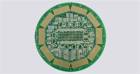
- Multi-Layer PCBs: These consist of multiple layers of conductive material separated by insulating layers. They are used in highly complex and dense electronic circuits, such as those found in computers and telecommunications equipment.
- Rigid PCBs: These are made from a solid substrate material that does not flex. They are used in applications where the PCB must maintain its shape and provide sturdy support.
- Flexible PCBs: These are made from flexible materials that allow the PCB to bend and twist. They are used in applications where space and weight are critical, such as in wearable technology and medical devices.
- Rigid-Flex PCBs: These combine rigid and flexible substrates, offering the benefits of both types. They are used in complex applications that require both durability and flexibility.
Materials Used in PCBs
The materials used in PCBs play a crucial role in their performance and durability. The primary materials include:
- Substrate: The base material of the PCB, typically made from fiberglass (FR4), which provides mechanical support and electrical insulation.
- Copper: Used to create the conductive pathways on the PCB. The thickness of the copper layer can vary depending on the current-carrying requirements of the circuit.
- Solder Mask: A protective layer applied over the copper traces to prevent oxidation and short circuits. It also provides insulation and improves the PCB’s durability.
- Silkscreen: A layer of ink used to print labels, component identifiers, and other information on the PCB. It aids in the assembly and troubleshooting process.
PCB Design Process
The design of a PCB is a critical step that determines its functionality and performance. The design process typically involves the following steps:
- Schematic Design: The first step is to create a schematic diagram that represents the electrical connections and components of the circuit. This diagram serves as a blueprint for the PCB layout.
- Component Placement: Once the schematic is complete, the next step is to place the components on the PCB layout. This involves determining the optimal arrangement of components to minimize signal interference and ensure efficient routing of traces.
- Routing: After component placement, the next step is to route the electrical connections (traces) between the components. This involves creating conductive pathways that connect the components according to the schematic diagram.
- Design Rule Check (DRC): Before finalizing the design, a Design Rule Check is performed to ensure that the layout complies with the manufacturing and electrical requirements. This step helps identify and correct any potential issues.
- Gerber File Generation: Once the design is finalized, Gerber files are generated. These files contain the necessary information for manufacturing the PCB, including the layout of the copper layers, solder mask, and silkscreen.
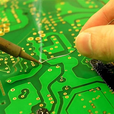
PCB Manufacturing Process
The manufacturing of PCBs involves several steps, each of which must be carefully controlled to ensure the quality and reliability of the final product. The main steps in the manufacturing process include:
- Substrate Preparation: The process begins with the preparation of the substrate material, typically fiberglass. The substrate is cut to the required size and cleaned to remove any contaminants.
- Copper Cladding: A thin layer of copper is laminated onto the substrate. This copper layer will be used to create the conductive pathways.
- Photoresist Application: A photoresist material is applied to the copper-clad substrate. This material is sensitive to light and will be used to transfer the PCB layout onto the copper layer.
- Exposure and Development: The photoresist-coated substrate is exposed to ultraviolet (UV) light through a photomask that contains the PCB layout. The exposed areas of the photoresist harden, while the unexposed areas remain soft and can be washed away.
- Etching: The substrate is then immersed in an etching solution that removes the unprotected copper, leaving behind the conductive pathways defined by the photoresist.
- Drilling: Holes are drilled into the substrate to accommodate through-hole components and vias (connections between different layers of the PCB).
- Plating: The drilled holes are plated with copper to create electrical connections between the layers of the PCB.
- Solder Mask Application: A solder mask is applied to the PCB to protect the copper traces and prevent short circuits. The solder mask is typically green, but other colors are also available.
- Silkscreen Printing: The final step is to apply the silkscreen layer, which includes labels, component identifiers, and other information.
- Testing and Inspection: The finished PCB is tested and inspected to ensure that it meets the required specifications and is free from defects.
Applications of PCBs
PCBs are used in a wide range of applications across various industries. Some of the most common applications include:
- Consumer Electronics: PCBs are found in virtually all consumer electronic devices, including smartphones, tablets, laptops, televisions, and gaming consoles.
- Automotive: Modern vehicles rely on PCBs for various functions, including engine control units, infotainment systems, and advanced driver-assistance systems (ADAS).
- Medical Devices: PCBs are used in medical devices such as pacemakers, imaging equipment, and diagnostic tools. The reliability and precision of PCBs are critical in these applications.
- Industrial Equipment: PCBs are used in industrial machinery and equipment for control, monitoring, and automation purposes.
- Aerospace and Defense: PCBs are used in aerospace and defense applications, including avionics, communication systems, and radar equipment. These PCBs must meet stringent reliability and performance standards.
- Telecommunications: PCBs are essential components in telecommunications equipment, including routers, switches, and base stations.
- IoT Devices: The Internet of Things (IoT) relies on PCBs for the connectivity and functionality of smart devices, such as smart home appliances, wearable technology, and sensors.
Conclusion
Printed Circuit Boards (PCBs) are a cornerstone of modern electronics, enabling the development of complex and compact electronic devices. From their early beginnings in the 20th century to their widespread use in today’s technology-driven world, PCBs have evolved significantly in terms of design, materials, and manufacturing processes. Understanding the different types of PCBs, the materials used, and the design and manufacturing processes is essential for anyone involved in the electronics industry. As technology continues to advance, PCBs will undoubtedly play an even more critical role in shaping the future of electronics.