Advanced Prototype PCB Assembly Strategies for Optimal Performance
Key Takeaways
Successful PCB assembly relies on balancing precision, efficiency, and scalability. At the core of high-quality PCBA, design validation ensures that prototypes meet both functional and manufacturability requirements. Rigorous precision manufacturing techniques, such as laser-drilled microvias and controlled impedance routing, minimize signal loss and enhance reliability. Streamlined workflows further optimize outcomes by integrating automated pick-and-place systems with real-time quality checks, reducing human error.
Critical component selection—prioritizing temperature-rated ICs and low-ESR capacitors—directly impacts performance under stress. Equally vital are testing protocols like automated optical inspection (AOI) and in-circuit testing (ICT), which identify flaws before deployment. For cost-sensitive projects, modular PCB assembly approaches allow iterative refinements without compromising timelines.
Furthermore, thermal management strategies, including optimized copper pours and heatsink integration, prevent overheating in dense layouts. By aligning PCBA processes with scalable design frameworks, teams can adapt to evolving complexity while maintaining consistency. These principles form a foundation for achieving first-pass success in prototype development, ensuring reliability from concept to production.

Precision Techniques for Reliable PCB Prototypes
Achieving reliability in PCB assembly requires meticulous attention to manufacturing tolerances and process controls. Modern precision techniques leverage laser-direct imaging (LDI) for sub-20μm trace accuracy and automated optical inspection (AOI) systems to detect microscopic defects. For PCBA prototypes, solder paste deposition methods like step-stencil printing ensure consistent volume across fine-pitch components, reducing short circuits and cold joints.
Tip: Implement design-for-manufacturability (DFM) checks early to identify potential fabrication issues, such as insufficient annular ring clearance or thermal imbalances.
Critical factors in reliable prototyping include:
| Technique | Tolerance Range | Application |
|---|---|---|
| Laser drilling | ±5μm | HDI/microvia PCBs |
| Selective soldering | ±0.1mm | Mixed-technology components |
| Conformal coating | 25–75μm | Environmental protection |
Advanced PCB assembly workflows now integrate 3D X-ray inspection to validate BGA and QFN solder joints, which are invisible to traditional AOI systems. For PCBA designs requiring high-frequency performance, impedance-controlled routing and substrate material selection (e.g., Rogers 4350B) minimize signal loss. Thermal management strategies, such as embedded copper coins or via-in-pad structures, further enhance reliability by dissipating heat efficiently. By combining these precision methods, engineers can reduce iteration cycles while ensuring prototypes meet performance benchmarks.
Streamlining PCB Prototype Workflows
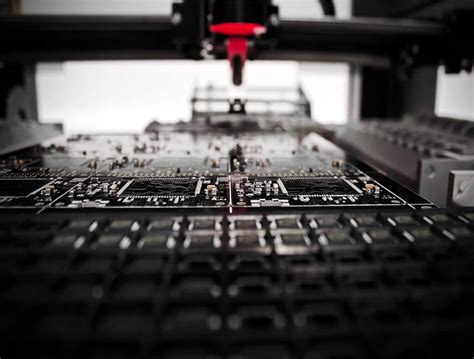
Modern PCB assembly processes require meticulous coordination between design and production phases to achieve optimal prototype performance. Implementing design for manufacturability (DFM) checks early in development prevents costly revisions, ensuring board layouts align with PCBA capabilities. Automated pick-and-place systems coupled with optical inspection tools accelerate component placement while maintaining sub-100-micron accuracy – critical for high-density interconnect designs.
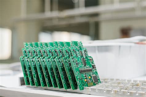
By adopting standardized assembly templates for recurring prototype types, engineers reduce setup time by up to 40%, particularly for mixed-technology boards combining SMT and through-hole components. Advanced facilities integrate real-time inventory tracking with PCB assembly workflows, automatically adjusting material orders based on project pipelines.
For complex prototypes, modular PCBA approaches enable parallel processing of functional blocks, compressing lead times without compromising testing rigor. Transitioning to paperless workflow systems with barcode scanning eliminates documentation errors that account for 12% of prototype delays, according to IPC-9151 process data. When combined with just-in-time material delivery strategies, these optimizations create a cohesive production environment where design iterations progress seamlessly from CAD models to functional prototypes.
Component Selection Tips for Optimal PCB Assembly
Strategic component selection forms the foundation of high-performing PCB assembly processes, directly impacting functionality, durability, and manufacturability. Begin by prioritizing thermal compatibility between components and substrate materials to prevent failures under operational stress. For instance, high-power devices demand materials with low thermal resistance, while low-power circuits benefit from cost-effective alternatives.
When sourcing parts for PCBA, verify footprint accuracy to ensure alignment with design files, minimizing placement errors during automated assembly. Opt for industry-standard packages (e.g., QFN, BGA) to streamline soldering and inspection workflows. Additionally, evaluate supplier reliability by cross-referencing lead times, certifications, and batch consistency—critical for avoiding delays in prototyping cycles.
Equally critical is balancing performance with scalability. Select components rated for extended temperature ranges and higher tolerances if the design targets harsh environments. For mixed-signal boards, prioritize low-noise amplifiers and shielded connectors to preserve signal integrity. Finally, leverage simulation tools to model electrical behavior pre-assembly, identifying mismatches early. By integrating these practices, engineers ensure PCB assembly outcomes align with both prototype objectives and long-term reliability goals.
Testing Protocols for High-Performance PCB Prototypes
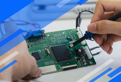
Effective PCB assembly processes require rigorous testing protocols to ensure prototypes meet design specifications and operational demands. Modern PCBA workflows integrate automated optical inspection (AOI) and X-ray testing to detect soldering defects, component misalignment, or micro-cracks invisible to the naked eye. These non-destructive methods preserve prototype integrity while validating assembly accuracy.
For high-frequency or high-power applications, signal integrity testing becomes critical. Engineers employ vector network analyzers to assess impedance matching and trace performance, minimizing signal loss in advanced PCB assembly designs. Environmental stress tests, including thermal cycling and vibration simulations, further validate prototypes under extreme operating conditions.
Transitioning from design to production, in-circuit testing (ICT) verifies electrical connectivity and component functionality, ensuring no latent defects persist. Pairing ICT with boundary-scan techniques streamlines fault isolation in densely packed PCBA layouts. By aligning these protocols with industry standards like IPC-A-610, manufacturers systematically eliminate risks while maintaining compliance with reliability benchmarks.
Implementing a phased testing approach—from pre-assembly material checks to post-production validation—creates a feedback loop that refines both design and PCB assembly processes. This structured methodology not only accelerates time-to-market but also establishes a foundation for scalable manufacturing of complex prototypes.

Efficiency-Driven PCB Prototype Assembly Tactics
Achieving peak efficiency in PCB assembly requires strategic integration of automation and process optimization. Modern PCBA workflows leverage automated pick-and-place systems to accelerate component placement while minimizing human error, particularly critical for high-density prototypes. Implementing lean manufacturing principles—such as just-in-time material sourcing and batch-size reduction—ensures resource allocation aligns with project timelines without compromising quality.
Advanced assembly lines now employ real-time monitoring systems to track solder paste application accuracy and reflow oven profiles, enabling immediate adjustments during PCB assembly. Pairing this with design-for-manufacturability (DFM) checks early in the prototyping phase reduces iterative rework by up to 30%. For instance, optimizing pad layouts for automated soldering or selecting standardized component footprints streamlines PCBA processes.
Transitioning to modular tooling setups further enhances adaptability, allowing rapid configuration changes between prototype batches. This approach not only shortens lead times but also supports scalability for transitioning from low-volume prototypes to pilot production. By balancing speed with precision, engineers ensure that efficiency gains in PCB assembly directly translate to reliable, high-performance electronic prototypes.
Cost-Effective Strategies in PCB Prototype Manufacturing
Achieving cost efficiency in PCB assembly requires balancing performance goals with budgetary constraints. A foundational step involves optimizing design files for manufacturability—leveraging Design for Manufacturing (DFM) principles to minimize material waste and reduce production errors. For instance, standardizing pad sizes and avoiding overly complex via structures can lower fabrication costs while maintaining reliability.
Material selection plays a pivotal role in cost management. While high-performance substrates like Rogers or polyimide are ideal for specialized applications, cost-effective alternatives such as FR-4 or aluminum-backed PCBs often suffice for early-stage prototypes. Partnering with suppliers who offer bulk pricing for common components, such as resistors or ICs, further trims expenses without compromising PCBA quality.
Automation is another critical lever. Integrating pick-and-place machines and reflow ovens into the PCB assembly workflow reduces manual labor costs and accelerates turnaround times. For prototypes requiring iterative testing, modular designs enable selective upgrades, avoiding full-board replacements. Additionally, adopting automated optical inspection (AOI) early in the process identifies defects before they escalate into costly rework.
Finally, scalability should be embedded into prototype strategies. Designing with future mass production in mind—such as using standardized footprints or avoiding obsolete parts—ensures seamless transitions to larger batches. By aligning PCBA workflows with lean manufacturing principles, engineers can deliver high-performing prototypes that align with both technical and financial objectives.
Ensuring Reliability Through Advanced PCB Assembly
Achieving consistent reliability in PCB assembly requires integrating cutting-edge techniques with rigorous quality control measures. Modern high-density interconnect (HDI) designs demand precision in PCBA processes, where even minor deviations in solder paste application or component placement can compromise performance. Implementing automated optical inspection (AOI) systems during assembly ensures early detection of defects like misaligned components or insufficient solder joints, reducing post-production failures.
Thermal management plays a pivotal role in reliability, particularly for prototypes intended for harsh environments. Using thermal cycling tests during PCB assembly validates the board’s resilience to temperature fluctuations, while advanced materials like high-Tg substrates enhance stability under prolonged stress. Additionally, employing conformal coating techniques protects sensitive circuits from moisture, dust, and chemical exposure, extending the lifespan of the PCBA.
To maintain signal integrity, controlled impedance routing and EMI shielding are prioritized in multilayer designs. Pairing these strategies with design for manufacturability (DFM) principles ensures seamless transitions from prototyping to full-scale production. By combining meticulous process controls with innovative materials, engineers can deliver PCB assemblies that meet stringent reliability standards across diverse applications.
Scalable Solutions for Complex PCB Prototype Designs
Navigating intricate PCB assembly requirements demands solutions that adapt to evolving design complexities while maintaining production scalability. For multi-layered or high-density interconnect (HDI) prototypes, adopting modular design frameworks enables seamless integration of additional functionalities without compromising existing layouts. This approach ensures PCBA processes remain efficient even as component counts or circuit density increases.
Leveraging design-for-manufacturing (DFM) principles early in the development cycle minimizes rework risks. For instance, standardizing pad sizes and trace widths across modules simplifies automated PCB assembly, allowing manufacturers to scale production without sacrificing precision. Advanced pick-and-place systems paired with solder paste inspection (SPI) tools further enhance repeatability, critical for prototypes transitioning to mid-volume runs.
Scalability also hinges on flexible material selection. Opting for substrates with compatible thermal and mechanical properties ensures consistent performance across varying design iterations. Additionally, integrating testability features like boundary scan or built-in self-test (BIST) circuits accelerates validation, reducing bottlenecks in high-mix PCBA environments. By aligning design complexity with manufacturing agility, teams can achieve both technical excellence and operational adaptability in prototype development.
Conclusion
Effective PCB assembly strategies culminate in prototypes that balance performance, reliability, and cost-efficiency. By integrating precision PCBA methodologies with rigorous testing frameworks, engineers ensure that prototypes meet exacting standards while minimizing iterative delays. Emphasizing component compatibility and thermal management during assembly not only enhances functionality but also extends the lifecycle of electronic systems.
A streamlined workflow, supported by automated PCB assembly tools, reduces human error and accelerates time-to-market. Additionally, adopting scalable design principles allows seamless adaptation to evolving project requirements, whether for low-volume prototypes or complex multi-layer boards. Prioritizing data-driven validation—through in-circuit testing and functional diagnostics—ensures defects are identified early, safeguarding against costly revisions.
Ultimately, the synergy between advanced PCBA techniques and strategic planning transforms prototype development into a repeatable, high-yield process. As technology advances, staying ahead demands continuous refinement of assembly practices, ensuring prototypes not only meet current benchmarks but also anticipate future innovation.
Frequently Asked Questions
What distinguishes prototype PCB assembly from standard production runs?
Prototype PCB assembly focuses on low-volume, high-precision builds to validate designs before mass production. This stage emphasizes rigorous functional testing and iterative adjustments, whereas standard runs prioritize scalability and cost efficiency.
How does component selection impact prototype reliability?
Choosing high-quality components with verified specifications ensures stable performance in PCBA prototypes. Factors like thermal tolerance and signal integrity directly affect reliability, especially in complex designs requiring tight tolerances.
What testing protocols are critical for prototype validation?
Advanced PCB assembly workflows integrate automated optical inspection (AOI) and in-circuit testing (ICT) to detect soldering defects or electrical inconsistencies. Environmental stress testing further validates durability under extreme conditions.
Can cost-effective strategies compromise prototype quality?
Balancing cost and quality requires optimizing material sourcing and leveraging modular PCBA designs. Techniques like panelization reduce waste, while simulation tools minimize physical iterations without sacrificing performance.
How do streamlined workflows enhance assembly efficiency?
Adopting design for manufacturability (DFM) principles reduces rework risks. Automated pick-and-place systems and standardized bill of materials (BOM) templates accelerate turnaround times for prototype PCB assembly.
What scalability challenges arise in complex PCB prototypes?
High-density interconnects (HDI) and mixed-signal layouts demand precise layer stackup planning. Modular PCBA architectures and cross-functional collaboration ensure scalability without compromising signal integrity.
Ready to Optimize Your Prototype PCB Assembly?
Explore our advanced solutions for PCB assembly and PCBA services tailored to your project’s needs. Please click here to consult with our engineering team and streamline your prototyping process.