Layer PCB Manufacturing: Expert Stack-Up Design Solutions
Key Takeaways
When navigating PCB manufacturing for multilayer designs, understanding core technical and operational factors ensures optimal outcomes. Stack-up design directly impacts signal integrity and thermal performance—critical for high-speed or high-frequency applications. Leading PCB manufacturing companies prioritize custom layer configurations to address impedance control and electromagnetic interference, particularly in 10-layer boards where alternating signal and plane layers enhance noise reduction.
Balancing PCB manufacturing cost with performance requires strategic material choices. For instance, selecting low-loss laminates like Rogers or Isola FR-4 (https://www.andwinpcba.com)) minimizes signal degradation but may increase expenses. To mitigate this, work with partners offering design-for-manufacturability (DFM) analysis to avoid over-engineering.
Tip: Always validate stack-up proposals with your manufacturer early in the design phase—this reduces revisions and aligns expectations for high-density interconnects.
In the PCB manufacturing business, reliability hinges on precise layer alignment and via structures. Buried and blind vias in 10-layer designs improve routing density but demand advanced drilling techniques. Streamlined production workflows, paired with rigorous testing protocols, ensure consistent quality across batches while meeting tight timelines. By aligning technical specifications with commercial realities, you can optimize both functionality and scalability in multilayer PCB projects.

-Layer PCB Manufacturing Essentials
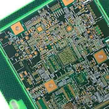
When designing multilayer PCBs, understanding PCB manufacturing fundamentals ensures your board meets performance and reliability standards. The number of layers directly impacts signal integrity, thermal management, and PCB manufacturing cost, making stack-up design a critical consideration. For instance, a 10-layer configuration often balances high-density routing with controlled impedance, but this requires precise material selection and alignment between PCB manufacturing companies and design teams.
Here’s a breakdown of key factors influencing multilayer builds:
| Layer Count | Typical Use Case | Complexity | Cost Impact |
|---|---|---|---|
| 4-6 Layers | Consumer electronics | Moderate | Low-Medium |
| 8-10 Layers | Networking/Industrial | High | Medium-High |
| 12+ Layers | Aerospace/Defense | Very High | High |
To optimize PCB manufacturing business outcomes, prioritize dielectric materials with low loss tangents for high-speed signals and ensure symmetrical layer stacking to prevent warping. Advanced PCB manufacturing processes like laser-drilled microvias enable tighter interlayer connections, but these add to production time and cost. Always collaborate with suppliers early to align design choices with fabrication capabilities—this avoids rework and ensures your high-density circuits perform as intended without exceeding budget constraints.
Balancing performance and affordability hinges on selecting the right layer count and materials for your application. For example, a 10-layer board might use alternating signal and ground planes to minimize EMI, but simpler designs could reduce layers to lower PCB manufacturing cost. Regular design-for-manufacturing (DFM) checks with your PCB manufacturing companies help identify potential issues like impedance mismatches or inadequate thermal reliefs before production begins.
Optimizing Signal Integrity with Stack-Ups
When designing multilayer PCBs, stack-up configuration directly impacts signal integrity and electromagnetic performance. Proper layer arrangement minimizes noise coupling and ensures controlled impedance for high-speed signals. PCB manufacturing companies often recommend symmetrical stack-ups with dedicated signal, power, and ground layers to reduce crosstalk and voltage fluctuations. For instance, placing high-speed traces between ground planes creates a shielding effect, while alternating dielectric materials can fine-tune signal propagation delays.
Balancing PCB manufacturing cost with performance requires strategic layer allocation. Thinner prepreg layers between critical signal layers lower capacitance, but tighter tolerances might increase production complexity. Reputable PCB manufacturing partners use simulation tools to validate stack-up designs before fabrication, ensuring compliance with impedance targets. This proactive approach prevents costly redesigns and aligns with the scalability needs of your PCB manufacturing business.
Transitioning between layers also demands attention to via placement and anti-pad sizing to avoid impedance discontinuities. By collaborating with experts who understand material properties and thermal management, you ensure that the final stack-up meets both electrical and mechanical reliability standards.
Custom Layer Configurations for Complex Circuits
When designing complex circuits, achieving optimal performance requires tailoring PCB manufacturing processes to your specific needs. Custom layer configurations enable you to address challenges like high-speed signal routing, power distribution, and EMI mitigation. Leading PCB manufacturing companies leverage advanced software to model stack-ups that balance impedance control, thermal management, and mechanical stability—critical for applications such as aerospace or IoT devices.
For multi-functional systems, you might need dedicated layers for high-frequency signals paired with shielding planes or split power domains. This precision reduces crosstalk and ensures signal integrity while minimizing PCB manufacturing cost through efficient material usage. However, adding layers isn’t always the answer—over-engineering can inflate expenses without tangible benefits. Instead, focus on strategic layer allocation: for example, placing sensitive analog traces on inner layers with ground shielding or using hybrid materials to manage heat in high-power sections.
Collaborating with experienced PCB manufacturing business partners ensures your design aligns with fabrication capabilities. They’ll guide you on trade-offs, such as choosing between low-loss substrates for RF circuits or cost-effective FR-4 for digital sections, ensuring reliability without compromising scalability. By prioritizing application-specific layer planning, you create boards that perform flawlessly under real-world conditions while maintaining production efficiency.
Advanced Materials in Multilayer PCB Design
When designing PCB manufacturing solutions for complex multilayer boards, material selection directly impacts performance, reliability, and PCB manufacturing cost. Modern high-frequency laminates, such as Rogers or Isola substrates, minimize signal loss in high-speed applications, while low-loss prepregs ensure consistent dielectric properties across layers. For thermal management, PCB manufacturing companies often integrate ceramic-filled or metal-core materials to dissipate heat in power-dense circuits, preventing delamination and extending product lifespan.
Balancing material performance with economic feasibility requires expertise. For instance, polyimide films offer exceptional thermal stability for aerospace applications but increase PCB manufacturing business expenses compared to standard FR-4. Hybrid stack-ups—combining specialty and conventional materials—let engineers optimize cost without compromising critical functions like impedance control or EMI shielding.
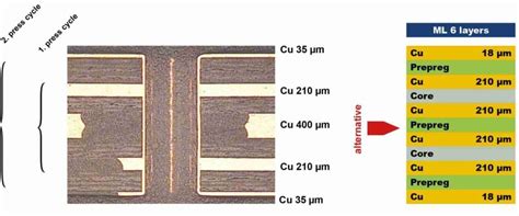
This becomes particularly critical in 10-layer designs, where layer count amplifies material-related challenges. Advanced adhesives and copper foils with ultra-low profile surfaces further enhance signal integrity in high-density interconnects. By partnering with suppliers who provide certified material data, you ensure compliance with industry standards while avoiding costly redesigns. Ultimately, the right material strategy not only meets technical demands but also aligns with your project’s budgetary constraints—a key differentiator among leading PCB manufacturing companies.
Expert Solutions for 10-Layer PCB Stack-Ups
When designing complex 10-layer PCBs, you need stack-up configurations that balance performance requirements with PCB manufacturing cost considerations. Expert PCB manufacturing companies achieve this through precise layer arrangement, combining signal integrity priorities with thermal management and power distribution needs. Advanced materials like high-speed laminates or low-loss dielectrics are strategically placed in critical layers to minimize signal loss while maintaining mechanical stability.
Experienced engineers optimize PCB manufacturing business workflows by implementing hybrid via structures (blind/buried vias) to conserve board space in high-density designs. They also leverage simulation tools to validate impedance control and EMI shielding effectiveness before production. For high-speed digital circuits or RF applications, staggered layer sequencing might be recommended to reduce cross-talk between adjacent signal layers.
To maintain reliability, strict adherence to manufacturing tolerances is enforced during layer alignment and lamination processes. Trusted suppliers often provide stack-up validation services, identifying potential warpage risks or material compatibility issues early. This proactive approach streamlines PCB manufacturing timelines while preventing costly redesigns in later stages.
Balancing Cost and Performance in PCB Layers
When designing multilayer PCBs, striking the right balance between pcb manufacturing cost and performance requires careful planning. While adding layers improves signal integrity and power distribution, each additional layer increases material expenses and complexity. High-density designs often demand more layers, but pcb manufacturing companies recommend optimizing stack-up configurations to avoid unnecessary costs. For example, using hybrid materials—combining standard FR-4 with high-speed substrates in critical areas—can reduce expenses without sacrificing performance.
To minimize pcb manufacturing business overhead, consider standardizing layer counts for similar projects or reusing proven stack-ups. However, overly aggressive cost-cutting risks compromising thermal management or EMI shielding. Advanced simulation tools help validate designs before production, ensuring layer arrangements meet both electrical and budgetary requirements. Partnering with manufacturers early in the design phase ensures alignment on cost-effective material choices and fabrication tolerances.
Ultimately, the goal is to align layer count with application needs. A 10-layer board might be ideal for a high-speed server but excessive for a consumer IoT device. By analyzing signal requirements and leveraging pcb manufacturing expertise, you can achieve robust performance while maintaining cost efficiency.
Key Considerations for 10-Layer Board Reliability
When designing a 10-layer PCB, ensuring long-term reliability requires balancing advanced engineering practices with meticulous material and process choices. PCB manufacturing companies prioritize thermal management to mitigate warping or delamination, especially in high-power applications. This starts with selecting substrates that match the board’s operational temperature range—for example, FR-4 for moderate environments or polyimide for extreme conditions.
Signal integrity hinges on precise stack-up configurations, where alternating power, ground, and signal layers minimize crosstalk and EMI. Impedance control becomes critical here, demanding tight tolerances during etching and lamination. For PCB manufacturing cost optimization, consider hybrid stack-ups that pair high-performance materials (like Rogers) with standard substrates in non-critical layers.
Durability also depends on via reliability. Microvias and filled vias reduce stress points in high-density designs, but their success relies on laser drilling accuracy and copper plating quality. Partnering with PCB manufacturing business experts ensures compliance with IPC-6012 Class 3 standards for harsh-environment applications.
Finally, thermal cycling tests and accelerated aging simulations validate design choices. These steps help identify weak points in solder joints or layer adhesion before mass production. By aligning your requirements with a manufacturer’s capabilities early, you avoid costly revisions and ensure the final product meets both performance and longevity goals.
Streamlined Production for High-Density PCBs
When dealing with high-density PCBs, streamlined production becomes critical to maintain precision while managing PCB manufacturing cost. Modern PCB manufacturing companies leverage automated processes like laser direct imaging (LDI) and automated optical inspection (AOI) to ensure tight tolerances for microvias and fine-pitch components. This approach minimizes human error, accelerates turnaround times, and scales efficiently—key factors for businesses balancing complex designs with budgetary constraints.
By integrating advanced material handling systems and dynamic panelization strategies, manufacturers optimize material usage, reducing waste in the PCB manufacturing business. For multilayer boards, sequential lamination cycles are carefully timed to prevent warpage or delamination, even under high thermal stress. Additionally, design-for-manufacturability (DFM) checks are embedded early in the workflow to preempt issues like impedance mismatches or insufficient copper balancing.
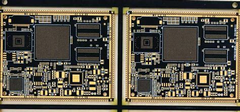
Moreover, high-density interconnects (HDI) require specialized drilling and plating techniques, which top-tier PCB manufacturing providers execute using controlled-depth drilling and filled via technologies. This ensures reliable layer transitions while maintaining signal integrity across densely packed traces. Ultimately, partnering with experts who prioritize process standardization alongside flexibility allows you to navigate the complexities of high-density PCB production without compromising scalability or reliability—especially vital for 10-layer configurations demanding rigorous layer alignment.
Conclusion
When evaluating PCB manufacturing for complex multilayer designs, the interplay between technical precision and economic feasibility becomes paramount. Choosing experienced PCB manufacturing companies ensures access to advanced stack-up engineering and material expertise, critical for balancing signal integrity with thermal management in high-density layouts. While PCB manufacturing cost often scales with layer count, strategic decisions in dielectric materials and via structures can optimize performance without unnecessary expenditure. For businesses scaling their PCB manufacturing business, prioritizing reliability testing and streamlined production workflows minimizes delays in high-volume orders. Ultimately, a 10-layer PCB’s success hinges on aligning design complexity with manufacturing capabilities—partnering with specialists who understand both the electrical and operational nuances ensures your project meets performance benchmarks while adhering to budget constraints.
Frequently Asked Questions
When should you consider 10-layer PCBs for your project?
High-density designs requiring advanced signal integrity and EMI shielding often demand 10-layer configurations. PCB manufacturing companies recommend this stack-up for applications like telecommunications or industrial automation, where precise layer arrangements optimize performance.
How does layer count affect pcb manufacturing cost?
While adding layers increases material and labor expenses, strategic stack-up design balances PCB manufacturing business budgets with technical requirements. Costs scale with layer complexity, but optimized designs reduce redundant vias or materials to offset expenses.
What materials ensure reliability in multilayer PCBs?
Leading PCB manufacturing partners use high-Tg FR-4, polyimide, or low-loss laminates for thermal stability. Material selection depends on operating environments and frequency requirements, with hybrid stack-ups often blending materials for optimal electrical and mechanical performance.
Can 10-layer PCBs meet tight production timelines?
Advanced PCB manufacturing companies leverage automated optical inspection (AOI) and laser drilling to streamline fabrication. While multilayer boards require precise alignment, modern processes ensure 10-layer prototypes ship within 2-3 weeks for most high-density applications.
How do you verify 10-layer board reliability?
Rigorous testing protocols—including impedance checks, thermal cycling, and cross-sectional analysis—are critical. Partner with PCB manufacturing experts who provide full design-for-manufacturability (DFM) reports to validate layer alignment and material compatibility.
Need a Custom 10-Layer PCB Solution?
Optimize your next project with precision stack-up design. For tailored PCB manufacturing services, please click here to consult our engineering team.