PCB Overlay: A Comprehensive Guide
Introduction
Printed Circuit Boards (PCBs) are the backbone of modern electronics, providing the necessary platform for electrical components to connect and function together. As technology advances, the complexity and density of PCBs have increased, leading to the development of various techniques to enhance their functionality and reliability. One such technique is PCB overlay, a critical process in the design and manufacturing of PCBs. This article delves into the concept of PCB overlay, its importance, types, materials, design considerations, and applications.
What is PCB Overlay?
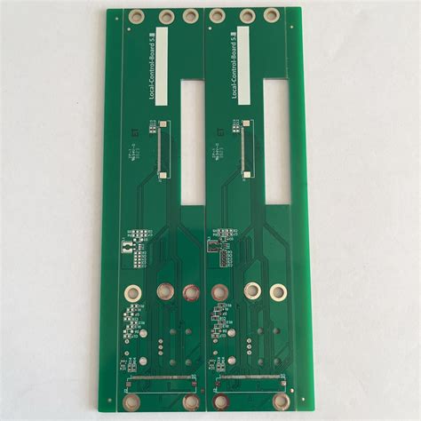
PCB overlay, also known as solder mask or solder resist, is a thin layer of polymer applied to the copper traces of a PCB. Its primary purpose is to protect the copper traces from oxidation, prevent solder bridges during the soldering process, and provide electrical insulation. The overlay also enhances the durability and reliability of the PCB by shielding it from environmental factors such as moisture, dust, and mechanical damage.
Importance of PCB Overlay
- Protection from Oxidation: Copper traces on a PCB are susceptible to oxidation when exposed to air, which can degrade their conductivity and lead to circuit failure. The overlay acts as a barrier, preventing oxygen from reaching the copper and thus preserving the integrity of the traces.
- Prevention of Solder Bridges: During the soldering process, molten solder can inadvertently create bridges between adjacent traces, causing short circuits. The overlay covers the areas where soldering is not required, ensuring that solder only adheres to the designated pads.
- Electrical Insulation: The overlay provides electrical insulation between the copper traces and any external conductive materials, reducing the risk of short circuits and electrical interference.
- Environmental Protection: The overlay shields the PCB from environmental factors such as moisture, dust, and chemicals, which can corrode the copper traces and compromise the board’s functionality.
- Aesthetic and Identification: The overlay can be colored (commonly green, but also available in other colors) and labeled with text or symbols, aiding in the identification of components and improving the overall appearance of the PCB.
Types of PCB Overlay
- Liquid Photoimageable Solder Mask (LPSM): This is the most common type of overlay, applied as a liquid and then cured using ultraviolet (UV) light. LPSM offers high resolution and is suitable for fine-pitch components.
- Dry Film Solder Mask (DFSM): DFSM is applied as a dry film and then laminated onto the PCB. It is less common than LPSM but offers better thickness control and is suitable for high-density interconnect (HDI) boards.
- Top and Bottom Overlay: PCBs typically have overlays on both the top and bottom layers. The top overlay covers the component side, while the bottom overlay covers the solder side.
- Selective Overlay: In some cases, only specific areas of the PCB require an overlay. Selective overlay involves applying the overlay only to those areas, leaving the rest of the board exposed.
Materials Used in PCB Overlay
- Epoxy-Based Resins: These are the most commonly used materials for PCB overlays due to their excellent adhesion, chemical resistance, and thermal stability.
- Acrylic-Based Resins: Acrylic overlays offer good flexibility and UV resistance but are less durable than epoxy-based overlays.
- Polyimide: Polyimide overlays are used in high-temperature applications due to their exceptional thermal stability and resistance to harsh environments.
- Silicone: Silicone overlays are flexible and resistant to extreme temperatures, making them suitable for specialized applications such as automotive and aerospace electronics.
Design Considerations for PCB Overlay
- Thickness: The thickness of the overlay is crucial for its effectiveness. Too thin, and it may not provide adequate protection; too thick, and it can interfere with component placement and soldering. Typical overlay thickness ranges from 0.5 to 2 mils (0.0127 to 0.0508 mm).
- Color: While green is the most common color for overlays, other colors such as red, blue, black, and white are also available. The choice of color can affect the visibility of components and labels, as well as the overall aesthetics of the PCB.
- Resolution and Alignment: High-resolution overlays are essential for fine-pitch components and high-density boards. Proper alignment during the application process is critical to ensure that the overlay covers the intended areas without encroaching on solder pads or vias.
- Thermal Management: The overlay material should have good thermal conductivity to dissipate heat generated by components, especially in high-power applications.
- Compatibility with PCB Materials: The overlay material must be compatible with the base material of the PCB (typically FR-4) and any other materials used in the board’s construction.
- Environmental Considerations: The overlay should be resistant to the environmental conditions the PCB will be exposed to, such as humidity, temperature extremes, and chemical exposure.
Application Process of PCB Overlay
- Cleaning: The PCB is thoroughly cleaned to remove any contaminants that could affect the adhesion of the overlay.
- Application: The overlay material is applied to the PCB using a variety of methods, including screen printing, spray coating, or curtain coating. For LPSM, the material is applied as a liquid and then exposed to UV light through a photomask to cure the desired areas.
- Curing: The overlay is cured using heat or UV light, depending on the material used. This process hardens the overlay and ensures it adheres firmly to the PCB.
- Inspection: The PCB is inspected to ensure the overlay is applied correctly, with no defects such as bubbles, voids, or misalignment.
- Finishing: Any excess overlay material is removed, and the PCB may undergo additional finishing processes such as surface plating or coating.
Applications of PCB Overlay
- Consumer Electronics: PCBs in smartphones, tablets, laptops, and other consumer electronics rely on overlays to protect their intricate circuits and ensure reliable performance.
- Automotive Electronics: Automotive PCBs are exposed to harsh conditions, including temperature extremes, vibration, and moisture. Overlays provide the necessary protection to ensure the longevity and reliability of these boards.
- Aerospace and Defense: In aerospace and defense applications, PCBs must withstand extreme conditions and rigorous performance standards. Overlays play a critical role in protecting these high-reliability boards.
- Medical Devices: Medical electronics require high levels of reliability and protection from environmental factors. Overlays help ensure the safe and effective operation of medical devices.
- Industrial Equipment: Industrial PCBs are often exposed to harsh environments, including chemicals, dust, and moisture. Overlays provide the necessary protection to maintain the functionality of these boards.
Challenges and Future Trends in PCB Overlay
- Miniaturization: As electronic devices continue to shrink, the demand for finer-pitch components and higher-density PCBs increases. This poses challenges for overlay application, requiring higher resolution and precision.
- High-Speed and High-Frequency Applications: The rise of high-speed and high-frequency electronics, such as 5G and IoT devices, demands overlays with low dielectric constants and low loss tangents to minimize signal interference.
- Environmental Regulations: Stricter environmental regulations are driving the development of eco-friendly overlay materials that are free from hazardous substances such as lead and halogen.
- Advanced Materials: Research is ongoing into new overlay materials with enhanced properties, such as improved thermal conductivity, flexibility, and resistance to extreme conditions.
- Automation and AI: The integration of automation and artificial intelligence in the PCB manufacturing process is expected to improve the precision and efficiency of overlay application, reducing defects and increasing throughput.
Conclusion
PCB overlay is a vital component in the design and manufacturing of modern electronics, providing essential protection and insulation for copper traces. As technology continues to evolve, the demands on PCB overlays will only increase, driving innovation in materials, application techniques, and design considerations. By understanding the importance, types, materials, and applications of PCB overlays, engineers and designers can ensure the reliability and performance of their electronic devices in an ever-advancing technological landscape.