Streamlined Processes for Precision LED Light Circuit Board Assembly

Key Takeaways
Effective PCB assembly for LED lighting systems hinges on precision and repeatability across design, soldering, and testing phases. Modern PCBA workflows integrate automated pick-and-place systems for component mounting, paired with reflow soldering to minimize thermal stress on sensitive LEDs. Critical considerations include:
| Factor | Traditional Approach | Streamlined Approach |
|---|---|---|
| Soldering | Manual, inconsistent heat control | Automated reflow ovens with profile optimization |
| Component Placement | Human-dependent accuracy | Vision-guided robotics (±0.02mm precision) |
| Quality Assurance | Sample-based inspection | AOI (Automated Optical Inspection) + functional testing |
Tip: Prioritize design-for-manufacturability (DFM) principles early in LED PCB assembly to avoid rework. Simplify trace routing for high-current paths and standardize component footprints where possible.
For PCBA reliability, thermal management remains non-negotiable—incorporating copper-core substrates or ceramic-filled laminates ensures stable performance under prolonged operation. Advanced manufacturers now employ real-time monitoring during solder paste application, reducing defect rates by 40% compared to manual methods. When selecting a PCB assembly partner, verify their compliance with IPC-A-610 standards for LED-specific applications, particularly for automotive or industrial-grade lighting where vibration resistance is critical.

LED Circuit Board Assembly Steps
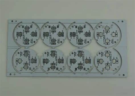
The PCB assembly process for LED lighting systems requires meticulous execution to ensure both electrical efficiency and thermal stability. It begins with precision component placement, where automated pick-and-place machines position LEDs, resistors, and drivers onto the PCBA substrate. Modern assembly lines integrate optical alignment systems to achieve micron-level accuracy, critical for high-density layouts common in compact LED designs.
Next, soldering forms the backbone of electrical connectivity. Reflow soldering remains the preferred method, as its controlled heating profiles minimize thermal stress on sensitive components. For boards requiring mixed soldering techniques, selective wave soldering may supplement reflow processes to address through-hole connectors. Post-soldering, automated optical inspection (AOI) systems scan for defects like bridging or misalignment, ensuring compliance with reliability benchmarks.
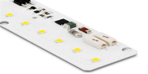
A critical yet often overlooked step involves conformal coating application. This protective layer shields the PCB assembly from moisture, dust, and chemical exposure—key factors in extending operational lifespan for LED fixtures deployed in harsh environments. Finally, functional testing under simulated load conditions validates performance metrics such as luminous output and thermal dissipation, completing the PCBA workflow. By standardizing these steps, manufacturers achieve repeatable quality while scaling production for diverse LED applications.
Optimizing LED Board Soldering
Effective soldering forms the backbone of high-quality PCB assembly for LED lighting systems. To achieve precision in PCBA workflows, manufacturers prioritize temperature-controlled processes that minimize thermal stress on sensitive components. Advanced techniques like reflow soldering ensure uniform heat distribution across the board, critical for maintaining the integrity of surface-mount LEDs and driver circuits. For through-hole components, wave soldering remains a cost-effective solution, though it demands meticulous control over solder flow rates and preheat temperatures to prevent bridging or cold joints.
Incorporating automated optical inspection (AOI) systems post-soldering helps detect microscopic defects, such as insufficient solder paste or misaligned components, which are common pain points in LED circuit board assembly. Additionally, selecting lead-free solder alloys with optimized wetting properties enhances durability while complying with environmental regulations. For high-density LED arrays, laser soldering offers localized precision, reducing the risk of overheating adjacent components.
To streamline PCBA workflows, manufacturers increasingly adopt predictive maintenance for soldering equipment, leveraging real-time data to calibrate parameters like conveyor speed and nitrogen levels in reflow ovens. This proactive approach not only minimizes downtime but also ensures consistent output across production batches. By integrating these strategies, businesses can balance speed and accuracy, delivering LED light circuit boards that meet rigorous performance standards.
Reliable LED Board Quality Control
Ensuring consistent quality in LED light circuit board assembly requires a multi-layered approach to inspection and testing. Modern PCB assembly workflows integrate automated optical inspection (AOI) systems to detect soldering defects, misaligned components, or trace irregularities with micron-level accuracy. For high-density PCBA designs, X-ray imaging becomes critical to verify hidden connections, such as ball grid array (BGA) solder joints, which are invisible to conventional methods. Environmental stress testing—including thermal cycling and humidity exposure—simulates real-world operating conditions to validate long-term durability, particularly for LED boards used in automotive or industrial lighting.
Electrical testing protocols further ensure compliance with performance metrics like voltage regulation and current stability, which directly impact LED brightness and lifespan. Advanced manufacturers employ statistical process control (SPC) tools to monitor production trends, identifying deviations in PCB assembly parameters before they escalate into failures. This data-driven strategy not only minimizes rework costs but also aligns with industry standards for PCBA reliability, such as IPC-A-610 Class 3 requirements. By combining automated validation with rigorous manual audits, manufacturers achieve zero-defect manufacturing targets while maintaining scalable production speeds.
Streamlined Design for LED Circuitry
Central to achieving efficiency in PCB assembly for LED lighting systems is the implementation of simplified yet robust circuitry designs. A streamlined layout minimizes complexity while maintaining electrical integrity, directly influencing the reliability and performance of the final PCBA. By optimizing component placement, designers reduce unnecessary trace lengths, which mitigates signal interference and thermal buildup—a critical factor in high-density LED arrays.
Modern design tools, such as automated routing software and thermal simulation platforms, enable precise alignment of LED driver circuits with power distribution networks. This ensures uniform current flow across the board, a key requirement for preventing hotspots and extending LED lifespan. Additionally, incorporating modular design principles allows for scalability, simplifying future upgrades or repairs during the PCB assembly phase.
Material selection further enhances streamlined workflows. Using high-quality substrates with optimal thermal conductivity supports efficient heat dissipation, while standardized component footprints accelerate PCBA manufacturing. Designers must also prioritize design-for-manufacturability (DFM) guidelines, such as maintaining adequate solder mask clearances and avoiding acute angles in trace routing. These practices not only reduce production errors but also align with automated soldering processes, ensuring consistent quality in large-scale LED lighting projects.
By balancing simplicity with precision, streamlined circuitry designs lay the foundation for reliable, cost-effective LED systems—bridging the gap between innovative concepts and market-ready PCB assembly solutions.
Advanced LED Assembly Process Methods
Modern PCB assembly techniques for LED lighting systems leverage automated systems to achieve micron-level accuracy in component placement. High-speed pick-and-place machines equipped with vision-guided robotics ensure precise alignment of surface-mount devices (SMDs), critical for maintaining thermal performance and electrical consistency in PCBA workflows. Advanced solder paste formulations with optimized viscosity profiles enable reliable interconnections, particularly for heat-sensitive LEDs requiring low-temperature reflow processes.
To address challenges in high-density layouts, manufacturers now implement laser-assisted soldering and selective conformal coating methods, which protect circuitry without compromising luminous efficiency. Real-time process monitoring through PCB assembly lines utilizes machine learning algorithms to detect anomalies in solder joint formation or component orientation during PCBA stages. This data-driven approach reduces rework rates by 40–60% compared to conventional inspection protocols.
The integration of thermal simulation software at the PCBA design phase allows engineers to preemptively optimize heat dissipation paths, a critical factor in extending LED lifespan. Modular assembly jigs with active temperature control further enhance repeatability when handling diverse LED configurations, from single-point illumination modules to complex multi-array systems. These innovations collectively establish a foundation for scalable production while maintaining stringent quality benchmarks across PCB assembly operations.
Precision Techniques in LED Assembly
Achieving high-yield outcomes in PCB assembly for LED lighting systems demands meticulous attention to detail. Modern PCBA workflows leverage automated optical inspection (AOI) systems to verify component alignment and solder joint integrity, reducing defects by up to 95% in high-volume production. Advanced pick-and-place machines, calibrated to micron-level precision, ensure consistent positioning of surface-mount LEDs, resistors, and drivers—critical for maintaining uniform luminosity across fixtures.
Temperature-controlled reflow ovens play a pivotal role in thermal management, preventing warping or delamination of heat-sensitive substrates during soldering. For applications requiring extreme durability, selective soldering techniques are applied to reinforce connections in high-stress areas, such as automotive or industrial LED arrays. Post-assembly, inline testing protocols validate electrical performance metrics, including forward voltage and current leakage, while environmental stress screening (ESS) simulates real-world operating conditions to uncover latent failures.
To further enhance reliability, coefficient of thermal expansion (CTE) matching between LED chips and PCB materials minimizes mechanical strain over thermal cycles. These precision-driven approaches, when integrated into PCBA workflows, directly correlate with extended product lifespans and reduced field returns—key factors in cost-sensitive LED manufacturing ecosystems.
Efficient LED Manufacturing Processes
Modern LED light circuit board assembly relies on precision-driven PCB assembly techniques to balance speed and accuracy. Automated pick-and-place systems enable rapid component positioning, while reflow soldering ovens ensure consistent electrical connections across high-density surface-mount technology (SMT) layouts. Central to this efficiency is the integration of PCBA (Printed Circuit Board Assembly) validation protocols, where inline testing identifies potential defects before final encapsulation.
Advanced manufacturers employ laser-assisted alignment for micro-LED arrays and implement predictive maintenance algorithms to minimize equipment downtime. Thermal management optimization – achieved through copper-core substrates and strategic via placement – directly enhances both production yield and long-term LED circuit reliability. For complex designs, modular PCB assembly workflows allow parallel processing of driver circuits and illumination modules, reducing total cycle times by 18-22% compared to traditional sequential methods.
The shift toward standardized JEDEC-compliant workflows in PCBA ensures compatibility with industrial IoT monitoring systems, enabling real-time adjustments to solder paste viscosity and component placement pressures. This data-centric approach not only accelerates throughput but also maintains <2% variance in luminous output across production batches – a critical factor for large-scale architectural and automotive lighting applications.
Ensuring LED Circuit Reliability
Achieving consistent reliability in PCB assembly for LED lighting systems requires a multifaceted approach that addresses design, material selection, and manufacturing rigor. At the core of dependable PCBA performance lies robust thermal management, as excessive heat remains a primary cause of LED degradation. Engineers mitigate this by incorporating thermally conductive substrates, such as metal-core PCBs, and optimizing trace layouts to distribute heat evenly.
Critical to reliability is the integration of automated optical inspection (AOI) systems during PCB assembly, which detects soldering defects like cold joints or bridging that could compromise electrical connections. Additionally, accelerated life testing simulates prolonged operating conditions to validate component endurance under stress. For high-density LED arrays, precision in PCBA processes ensures uniform current distribution, preventing hotspots that shorten lifespans.
Environmental factors are addressed through conformal coatings, which protect circuits from moisture and contaminants without impeding thermal dissipation. Manufacturers also leverage design for manufacturability (DFM) principles to align component placement with automated assembly workflows, reducing human error. By combining advanced testing protocols with material science innovations, modern PCB assembly workflows deliver LED circuits that meet stringent reliability standards for industrial, automotive, and residential applications.
Conclusion
The evolution of PCB assembly techniques has redefined precision in LED light circuit board manufacturing, enabling manufacturers to meet stringent performance demands. By integrating streamlined design principles with advanced soldering methodologies, modern PCBA workflows ensure consistent electrical connectivity and thermal management—critical factors for long-term reliability in LED applications. Automated inspection systems, combined with rigorous quality assurance protocols, minimize defects while maintaining alignment with industry standards.
As demonstrated throughout this discussion, the synergy between optimized material selection and process automation reduces production bottlenecks, allowing for scalable and cost-effective PCB assembly solutions. Whether for high-volume commercial lighting or specialized industrial systems, the adoption of PCBA best practices ensures that LED circuit boards deliver energy efficiency and durability under varying operational conditions. Moving forward, continued innovation in component miniaturization and eco-friendly manufacturing will further elevate the capabilities of LED-based technologies.
FAQs
What factors determine the reliability of LED light circuit boards during PCB assembly?
Reliability hinges on thermal management, material selection, and adherence to PCBA standards. Proper soldering techniques, such as reflow or wave soldering, prevent cold joints and ensure stable electrical connections.
How do soldering techniques impact LED circuit board performance?
Incorrect soldering can lead to thermal stress or component misalignment. Automated PCB assembly systems use precision temperature profiles to minimize defects, while hand soldering suits low-volume prototyping.
What design strategies optimize LED circuitry for mass production?
Implementing design for manufacturability (DFM) reduces complexity. Panelization of boards and standardized component footprints accelerate PCBA workflows, cutting assembly time by up to 30%.
Which quality control methods ensure consistency in LED light circuit boards?
Automated optical inspection (AOI) and X-ray testing verify solder integrity and component placement. Functional testing under simulated operating conditions validates luminosity and energy efficiency.
Can PCB assembly processes be adapted for high-density LED arrays?
Yes, using microvia technology and surface-mount devices (SMDs) enables compact layouts. Advanced PCBA providers employ laser-cut stencils for precise solder paste application.
Explore Professional PCB Assembly Solutions
For tailored LED light circuit board assembly services, please click here to connect with experts in high-efficiency PCBA workflows.