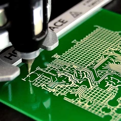
Streamlining PCB Development Through Additive Manufacturing Innovations
Key Takeaways
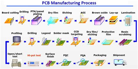
When exploring PCB manufacturing innovations, additive techniques offer distinct advantages that reshape traditional workflows. By integrating additive manufacturing (AM) into your processes, you can achieve faster iteration cycles, particularly for PCB manufacturing companies aiming to reduce time-to-market. Unlike conventional methods, AM eliminates the need for costly tooling, directly addressing PCB manufacturing cost concerns—especially for low-volume, high-complexity designs.
| Factor | Additive Manufacturing | Traditional Methods |
|---|---|---|
| Prototyping Speed | Days | Weeks |
| Design Complexity | High (multi-layer) | Moderate |
| Material Waste | Minimal | Significant |
| Tooling Costs | None | High |
For PCB manufacturing business models, this shift means enhanced flexibility in handling iterative testing and custom geometries. You can prototype intricate multi-layer configurations without renegotiating supplier timelines, while maintaining compatibility with established fabrication steps. However, AM isn’t a full replacement—it complements conventional techniques by bridging gaps in rapid development. By strategically blending both approaches, you optimize resource allocation and unlock new design possibilities without compromising scalability.
Additive Manufacturing Benefits for PCBs
By adopting additive manufacturing for PCB manufacturing, you gain unprecedented design flexibility while reducing PCB manufacturing cost. Unlike traditional subtractive methods, which often require multiple tooling steps, additive techniques build circuits layer by layer, enabling intricate layouts and material-efficient production. This approach is particularly advantageous for PCB manufacturing companies aiming to prototype complex designs rapidly—cutting development cycles from weeks to days.
The ability to iterate quickly means your PCB manufacturing business can test advanced configurations, such as embedded components or non-planar structures, without the overhead of conventional fabrication. For example, creating multi-layer boards with high-density interconnects becomes more feasible, as additive processes eliminate the need for excessive etching or drilling. Moreover, material waste drops significantly, aligning with sustainable practices that modern electronics demand.
Transitioning to additive methods doesn’t negate traditional processes but optimizes them. Hybrid workflows, where additive techniques handle prototyping and small batches, allow PCB manufacturing firms to scale efficiently. Recent studies show that integrating additive systems can reduce material usage by up to 70%, directly lowering PCB manufacturing cost for low-volume projects. This dual advantage of speed and precision positions additive manufacturing as a strategic tool for staying competitive in fast-paced electronics markets.
Multi-Layer PCB Designs via Additive Techniques
When designing multi-layer PCBs, traditional PCB manufacturing methods often struggle with intricate geometries and tight interlayer connections. Additive techniques, however, enable you to build complex layer stacks with precision, bypassing the limitations of subtractive processes like etching. By depositing conductive materials layer-by-layer, these methods reduce material waste and allow for embedded components—critical for high-density applications.
Tip: When exploring additive manufacturing for multi-layer designs, validate your design files early to avoid alignment issues between layers.
For PCB manufacturing companies, this approach slashes PCB manufacturing cost by minimizing tooling expenses and accelerating iteration cycles. Unlike conventional workflows requiring multiple photomasks, additive systems streamline prototyping, letting you test advanced architectures without upfront investments in specialized equipment. This flexibility is particularly valuable for startups or businesses scaling their PCB manufacturing business, as it lowers barriers to producing sophisticated boards.
The ability to integrate passive components (e.g., resistors, antennas) directly into layers further optimizes space and performance. While additive methods complement—not replace—traditional fabrication for mass production, they empower engineers to push the limits of miniaturization and functionality. By adopting these innovations, you can address evolving demands in IoT, wearables, and aerospace electronics, where compact, multi-functional designs are non-negotiable.
Rapid Prototyping for Complex Electronics
When designing intricate electronic systems, you often face challenges in validating PCB manufacturing concepts quickly and cost-effectively. Additive manufacturing addresses this by enabling on-demand prototyping of multi-layer boards with embedded components or unconventional geometries. Unlike traditional workflows that require weeks of tooling adjustments, PCB manufacturing companies using additive techniques can iterate designs in days—or even hours—by bypassing photolithography and etching steps. This agility becomes critical when testing high-density interconnects or flexible circuits for wearables, where even minor errors in layer alignment can derail projects.
By reducing material waste and labor-intensive processes, additive methods also lower PCB manufacturing cost for prototypes, allowing engineers to explore more design variations without exceeding budgets. For instance, functional testing of a 12-layer board with microvia arrays becomes economically feasible when layers are printed sequentially rather than laminated in bulk. While additive systems won’t replace mass production yet, they’re reshaping the PCB manufacturing business by accelerating time-to-market for specialized applications like IoT sensors or aerospace electronics. This hybrid approach—combining rapid prototyping with scaled traditional fabrication—ensures you stay competitive in markets demanding both innovation and reliability.
Accelerating Production Cycles with AM
When optimizing PCB manufacturing timelines, additive manufacturing (AM) introduces agile workflows that compress development phases by weeks. Unlike traditional methods requiring photomasks and chemical etching, AM builds multi-layer boards directly from digital files, bypassing tooling delays. This enables PCB manufacturing companies to shift from batch processing to just-in-time production, particularly beneficial for low-volume, high-complexity designs.
By eliminating tooling steps, you reduce PCB manufacturing cost while maintaining precision—critical when iterating prototypes or addressing last-minute design changes. For instance, AM systems can produce functional boards within hours, allowing engineers to test and refine circuits same-day. This acceleration directly impacts your PCB manufacturing business by enabling faster client turnarounds and more competitive bids for time-sensitive projects.
Moreover, AM’s compatibility with hybrid approaches lets you combine additive layers with conventional processes, balancing speed and performance. Transitioning to this model doesn’t require abandoning existing infrastructure; instead, it augments capacity during peak demand. The result? A streamlined pipeline where design validation, production, and delivery operate in tighter synchrony—key for staying ahead in industries like IoT or aerospace, where PCB manufacturing timelines dictate market success.
Complementing Traditional PCB Fabrication
While additive manufacturing introduces groundbreaking efficiencies, it’s not positioned to replace conventional PCB manufacturing methods entirely. Instead, it acts as a strategic enhancer, addressing gaps where traditional techniques face limitations. For instance, subtractive processes like etching remain cost-effective for high-volume production, but they struggle with ultra-fine geometries or embedded components. Here, additive techniques excel, enabling PCB manufacturing companies to prototype intricate designs without retooling entire production lines.
This hybrid approach optimizes PCB manufacturing cost by reducing material waste and minimizing downtime during design iterations. Imagine validating a multi-layer board with embedded sensors in days rather than weeks—traditional fabrication would require multiple tooling cycles, while additive methods let you iterate digitally. For businesses balancing speed and precision, combining both workflows ensures scalability. You retain the reliability of established PCB manufacturing business models while unlocking agility for custom or low-volume projects.
Critically, additive manufacturing doesn’t disrupt supply chains—it integrates seamlessly. Companies can adopt it incrementally, using it for rapid validation before transitioning to mass production via traditional means. This flexibility is key for industries like aerospace or medical devices, where certification timelines demand both innovation and compliance. By blending the old and new, you future-proof operations without sacrificing what already works.
Additive Manufacturing for Advanced Electronics
When exploring advanced electronics, you’ll find that additive manufacturing is reshaping how PCB manufacturing companies approach intricate designs. Unlike subtractive methods, which often involve material waste and longer lead times, layer-by-layer fabrication allows for precise integration of high-density interconnects and embedded components. This capability is particularly valuable for prototyping multi-functional systems, where traditional PCB manufacturing cost structures struggle to balance precision and affordability.
By adopting additive techniques, you can bypass many constraints of conventional processes—such as photolithography limitations—while maintaining compatibility with existing materials like conductive polymers. For PCB manufacturing business models focused on low-volume, high-complexity projects, this translates to faster design iterations and reduced material waste. Moreover, additive methods enable on-demand production, letting you test functional prototypes within days rather than weeks.
However, integrating additive manufacturing doesn’t negate the role of traditional fabrication. Instead, it complements high-volume production lines by handling specialized tasks like creating 3D-printed circuitry for wearable tech or IoT devices. This hybrid approach ensures scalability, allowing you to optimize PCB manufacturing workflows without overhauling established infrastructure. As industries demand lighter, more compact electronics, additive technologies position your operations at the forefront of innovation—balancing agility with cost efficiency.
Enhancing Design Flexibility in PCBs
Additive manufacturing reshapes how you approach design constraints in PCB manufacturing, offering unprecedented freedom to experiment with geometries that traditional methods struggle to replicate. Unlike subtractive processes, which rely on etching predefined patterns, layer-by-layer fabrication allows you to create intricate traces, embedded components, and non-planar structures without costly tooling changes. This flexibility is particularly valuable for PCB manufacturing companies developing high-density interconnects or compact devices where space optimization is critical.
By integrating additive techniques, you can rapidly iterate designs to test functionality or adapt to evolving specifications—reducing PCB manufacturing cost associated with multiple prototype cycles. For instance, conductive inks and advanced substrates enable hybrid designs that merge rigid and flexible sections in a single build, eliminating the need for separate assembly steps. This capability not only accelerates time-to-market but also opens opportunities for PCB manufacturing business models centered on customized, low-volume production.
Transitioning to additive methods doesn’t mean abandoning conventional processes. Instead, it complements them by addressing niche challenges—like creating ultra-thin layers or embedding passive components—while maintaining compatibility with existing workflows. The result? A harmonized approach where design creativity meets practical scalability, empowering you to push the boundaries of what’s possible in modern electronics.
Conclusion
As you evaluate the evolving landscape of PCB manufacturing, additive techniques offer a strategic advantage for balancing innovation with practicality. By integrating rapid prototyping into your workflow, PCB manufacturing companies can reduce iterative design delays and validate complex geometries before committing to traditional fabrication. This hybrid approach not only optimizes PCB manufacturing cost but also extends the capabilities of conventional methods, particularly for low-volume, high-complexity projects.
The agility of additive manufacturing allows you to experiment with advanced materials and multi-layer configurations, fostering innovation without compromising scalability. For PCB manufacturing business models targeting niche markets or cutting-edge electronics, this flexibility becomes a competitive differentiator. While traditional processes remain essential for mass production, additive methods fill critical gaps in prototyping and specialized applications, ensuring your development pipeline stays responsive to market demands.
Ultimately, the synergy between additive and subtractive techniques creates a more resilient ecosystem for electronics development. By strategically leveraging both, you position your operations to adapt to emerging technologies while maintaining cost-efficiency across the product lifecycle.
Frequently Asked Questions
How does additive manufacturing reduce pcb manufacturing cost?
By eliminating tooling expenses and minimizing material waste, additive techniques allow pcb manufacturing companies to produce low-volume batches cost-effectively. This is particularly advantageous for prototyping complex geometries that would otherwise require expensive traditional setups.
Can additive methods replace conventional pcb manufacturing entirely?
Not yet. While AM excels at rapid prototyping and intricate designs, high-volume production still relies on traditional methods like etching. However, hybrid workflows combining both approaches optimize speed and scalability for pcb manufacturing business models.
What design freedoms does AM offer for multi-layer PCBs?
You can integrate embedded components and create non-planar circuits without the constraints of subtractive processes. This flexibility accelerates iterations, enabling pcb manufacturing companies to test advanced concepts faster than ever.
How does AM impact pcb manufacturing timelines?
Lead times shrink from weeks to days, as additive systems bypass multiple fabrication steps. This agility helps businesses respond to market changes swiftly, making pcb manufacturing cost structures more predictable for short-run projects.
Explore Advanced PCB Manufacturing Solutions
To see how additive innovations can enhance your electronics development, please click here for tailored pcb manufacturing strategies.