Layer PCB Prototypes With Blind Vias: Cost-Effective Solutions
Key Takeaways
When exploring PCB manufacturing options for 4-layer prototypes with blind vias, you’ll need to balance technical complexity and PCB manufacturing cost. While blind vias enhance signal integrity in dense designs, they require specialized expertise from PCB manufacturing companies. Prioritize suppliers that offer transparent pricing models to avoid hidden fees tied to via drilling depths or material grades.
Tip: Always request a cost breakdown from your supplier—details like via aspect ratios and layer alignment tolerances can significantly impact final expenses.
For budget-friendly outcomes, consider scaling down non-critical features (e.g., reducing via counts) without compromising performance. Many PCB manufacturing businesses now provide tiered pricing, letting you optimize costs for low-volume prototypes. However, fast-turnaround services might inflate expenses if design revisions occur mid-production.
To ensure reliability, verify certifications like ISO 9001 and IPC Class 2/3 standards. This step helps align PCB manufacturing cost with long-term quality, especially for complex multilayer boards. By collaborating early with engineers, you can identify cost-saving opportunities in material selection or panel utilization—key strategies for balancing affordability and functionality.
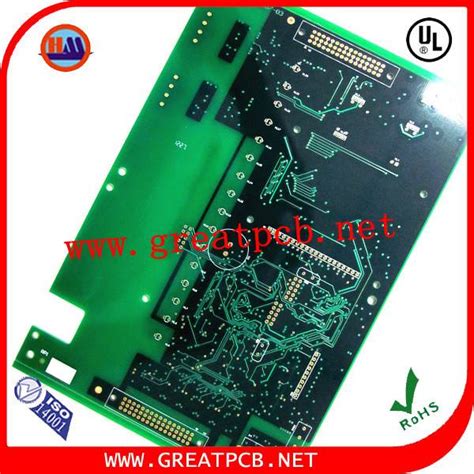
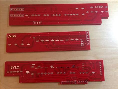
Affordable 4-Layer PCB Prototype Suppliers
When selecting PCB manufacturing companies for your 4-layer prototypes, balancing affordability with technical capabilities becomes critical. Reputable suppliers optimize PCB manufacturing cost by leveraging advanced processes like laser drilling for blind vias while maintaining quality standards. You’ll find that many global providers offer tiered pricing models—ideal for prototyping—where smaller batches avoid the overhead of mass production.
Consider these factors when evaluating suppliers:
| Criteria | Cost Impact | Key Considerations |
|---|---|---|
| Blind via technology | Adds 15–25% to base cost | Precision requirements for layer alignment |
| Material selection | FR-4 vs. high-frequency substrates | Thermal performance and signal integrity |
| Turnaround time | Expedited fees for <7-day delivery | Project deadlines vs. budget limits |
To reduce PCB manufacturing business expenses, prioritize suppliers offering design-for-manufacturability (https://www.andwinpcba.com) highlights how standardized via sizes can lower fabrication costs by up to 30%.
While negotiating pricing, confirm whether testing fees or tooling charges are included—these often appear as hidden costs in quotes. Partnering with PCB manufacturing specialists who automate processes (like AOI inspection) ensures consistent quality without inflating budgets. Always verify certifications like ISO 9001 or IPC Class 2/3 to align with your project’s reliability needs.
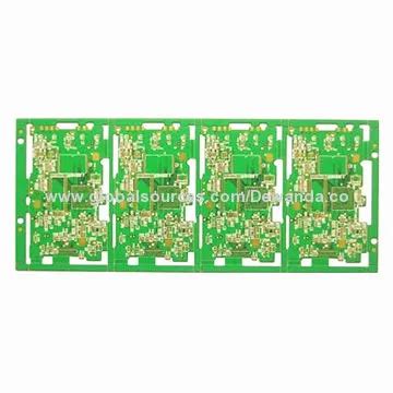
Global Manufacturers Offering Blind Vias
When selecting PCB manufacturing companies for prototypes requiring blind vias, you’ll find suppliers across Asia, North America, and Europe offering varying levels of cost efficiency and technical expertise. Asian manufacturers, for instance, often provide competitive PCB manufacturing cost structures due to scaled production capabilities, while European and North American suppliers emphasize precision and compliance with stringent quality standards. Balancing these factors becomes critical when your design demands blind vias—a feature that increases layer connectivity but can escalate expenses if not managed strategically.
Leading PCB manufacturing hubs like China and Taiwan specialize in high-volume prototyping with rapid turnaround times, making them ideal for projects where time-to-market is prioritized. Conversely, smaller regional suppliers in the U.S. or Germany might offer tighter tolerances for aerospace or medical applications, albeit at higher rates. To minimize PCB manufacturing business risks, verify certifications like ISO 9001 or IPC Class 3 compliance, especially when blind vias are essential for signal integrity in dense 4-layer boards.
Transitioning between regions requires evaluating hidden logistics costs, but global partnerships enable you to leverage economies of scale without sacrificing reliability. Some suppliers even provide hybrid models—combining offshore production with local quality audits—to optimize both PCB manufacturing cost and performance. Always request design-for-manufacturability (DFM) feedback early, as adjustments to via placement or layer stack-up can reduce fabrication complexity and unexpected charges.
Balancing Cost and Quality in PCB Prototypes
When evaluating PCB manufacturing options for 4-layer boards with blind vias, you’ll often face trade-offs between PCB manufacturing cost and performance. While advanced features like blind vias enhance signal integrity in complex designs, they can escalate expenses if not managed strategically. Reputable PCB manufacturing companies optimize this balance by leveraging standardized materials, streamlined processes, and bulk purchasing for common via sizes. For instance, selecting FR-4 substrates over high-frequency laminates reduces material costs without compromising functionality for most applications.
To minimize PCB manufacturing business overhead, prioritize suppliers offering design-for-manufacturing (DFM) analysis. This step identifies potential flaws early, preventing costly rework. Additionally, consolidating orders with manufacturers specializing in multilayer prototypes often yields volume discounts. However, ensure quality isn’t sacrificed—verify certifications like ISO 9001 and IPC Class 2/3 standards. Testing protocols, such as automated optical inspection (AOI), add marginal costs but safeguard against defects that could derail project timelines.
Ultimately, cost-effective prototyping hinges on transparent communication with your supplier. Clarify tolerances, layer alignment requirements, and via fill materials upfront to avoid unexpected charges. By aligning your design priorities with a manufacturer’s core capabilities, you can achieve reliable PCB manufacturing outcomes without overspending.
Reducing Expenses for Complex PCB Designs
When tackling intricate PCB designs, balancing PCB manufacturing cost with performance requires strategic planning. Start by evaluating PCB manufacturing companies that specialize in multilayer boards with blind vias—these suppliers often streamline processes to reduce overhead. For instance, consolidating layers through smart design software can minimize material waste, while standardized fabrication panels help distribute PCB manufacturing business expenses across multiple projects.
Design complexity directly impacts pricing, so simplify where possible. Use blind vias only in critical areas to avoid unnecessary drilling costs, and opt for manufacturers offering pooled engineering reviews to catch errors early. Many global PCB manufacturing providers now offer tiered pricing models, allowing you to scale production volumes without overcommitting budgets.
Another cost-saving tactic involves leveraging economies of scale. Partnering with suppliers that handle both prototyping and mass production reduces logistical friction and long-term PCB manufacturing cost. Always verify if hidden fees—like tooling charges or minimum order premiums—are baked into quotes. By aligning your design requirements with a manufacturer’s core capabilities, you avoid paying for underutilized services.
Finally, prioritize suppliers with transparent communication and proven expertise in 4-layer builds. A slight upfront investment in quality assurance often prevents costly redesigns, ensuring your project stays on budget and timeline.
Fast-Turnaround Solutions for Multilayer PCBs
When accelerating your PCB manufacturing timeline for complex multilayer designs, balancing speed with reliability is critical. Leading PCB manufacturing companies leverage advanced processes like automated panelization and high-precision laser drilling to reduce lead times for boards with blind vias or buried features. For projects requiring 4-layer prototypes, many suppliers now offer expedited 5-7 day services without compromising layer alignment or via integrity—key for high-frequency or dense circuitry.
To minimize PCB manufacturing cost during rushed orders, prioritize vendors with in-house material stock and streamlined logistics. Some providers bundle design-for-manufacturability (DFM) checks into their fast-track services, identifying potential flaws early to avoid costly respins. However, ensure signal integrity testing remains part of the workflow, even under tight deadlines.
For startups in the PCB manufacturing business, partnering with agile suppliers offering scalable batch sizes can prevent overstocking while meeting rapid iteration needs. Always verify certifications like ISO 9001 and IPC Class 2/3 to maintain quality benchmarks. By aligning your design specs with a manufacturer’s technical strengths, you secure both speed and functional reliability—a decisive edge in competitive hardware markets.
Hidden Costs in Blind Via PCB Production
When ordering PCB manufacturing services for designs requiring blind vias, you might focus on upfront quotes from PCB manufacturing companies, but overlooked expenses can inflate your final PCB manufacturing cost. For instance, material selection becomes critical with multilayer boards—using low-grade substrates to save money may lead to signal integrity issues, requiring costly redesigns. Similarly, via filling processes for blind vias often involve specialized equipment or adhesives, which some suppliers charge as add-ons.
Another hidden factor is testing complexity. While basic electrical tests are standard, advanced checks like impedance validation or thermal stress analysis might not be included in base pricing. This is especially true for PCB manufacturing business models prioritizing speed over thorough quality assurance. Additionally, rework rates tend to rise with intricate via structures—if a prototype fails due to via misalignment, delays and material waste compound expenses.
To mitigate these risks, clarify which services are bundled versus billed separately. Ask suppliers about their design-for-manufacturability (DFM) support to avoid layout errors upfront. Transparent PCB manufacturing companies often provide breakdowns of tooling, material, and testing fees, helping you anticipate true costs before committing.
Choosing Reliable PCB Prototype Services
When selecting a partner for PCB manufacturing, prioritize PCB manufacturing companies that demonstrate technical expertise in multilayer designs and blind via integration. Start by verifying certifications like ISO 9001 or UL listing, which signal adherence to industry standards. Reputable providers will openly share their PCB manufacturing cost structure, including material choices, layer stacking fees, and testing protocols—key factors for avoiding budget overruns.
Evaluate their track record with high-density interconnect (HDI) projects, as reliable PCB manufacturing business operations often highlight case studies or client testimonials for complex builds. Look for transparent communication on lead times and minimum order quantities (MOQs), especially if your project requires rapid iteration. A trustworthy supplier will also offer design-for-manufacturability (DFM) reviews to catch potential flaws early, reducing rework expenses.
Finally, balance affordability with accountability. While lower costs are tempting, ensure the provider uses quality laminates and follows IPC-A-600 standards for blind via reliability. Partnering with a certified manufacturer ensures your prototypes meet functional requirements without compromising scalability for future production runs.
Budget-Friendly 4-Layer Board Manufacturing
When sourcing PCB manufacturing services for 4-layer prototypes, prioritize suppliers that streamline production through standardized processes while maintaining precision. Many PCB manufacturing companies leverage economies of scale to reduce PCB manufacturing cost while accommodating blind vias, which are critical for compact designs. For instance, opting for optimized stack-ups and standard materials (like FR-4) instead of specialized substrates can lower expenses without compromising functionality.
To further control costs, consider design choices that minimize layer transitions and via complexities. While blind vias improve signal integrity in multilayer boards, their strategic placement reduces drilling and plating steps—key cost drivers in PCB manufacturing business workflows. Some manufacturers offer fixed panel utilization rates or shared tooling for prototype batches, effectively distributing setup costs across multiple orders.
However, balancing affordability with reliability requires verifying certifications like ISO 9001 or IPC Class 2/3 standards. Partnering with suppliers that provide detailed DFM (Design for Manufacturability) feedback ensures your design aligns with their production capabilities, avoiding costly revisions. By focusing on modular design practices and transparent pricing models, you can achieve cost-effective 4-layer prototypes without sacrificing performance.
Conclusion
When navigating PCB manufacturing for complex designs like 4-layer boards with blind vias, balancing cost-efficiency and technical precision is critical. Reputable PCB manufacturing companies often streamline processes to reduce PCB manufacturing cost without compromising quality, leveraging economies of scale or advanced fabrication techniques. While hidden expenses—such as material choices or additional testing—can impact budgets, partnering with certified suppliers ensures transparency and adherence to industry standards.
To optimize your PCB manufacturing business projects, prioritize vendors offering clear breakdowns of design-for-manufacturability (DFM) feedback and scalable production options. This approach minimizes rework delays and helps maintain tight timelines, especially for prototypes requiring fast turnaround. Remember, design complexity and lead times directly influence final costs, so iterative collaboration with your manufacturer is key. By aligning your requirements with a supplier’s core capabilities, you secure reliable, cost-effective solutions that meet both technical and budgetary goals.
Frequently Asked Questions
How do blind vias affect PCB manufacturing cost for 4-layer prototypes?
Blind vias add complexity to the PCB manufacturing process, requiring specialized drilling and plating. While this increases initial costs, partnering with experienced PCB manufacturing companies can optimize layer stacking and reduce waste, balancing expenses for high-quality outputs.
Can small-batch orders stay affordable with complex designs?
Yes. Many PCB manufacturing suppliers offer tiered pricing, allowing you to scale orders without overspending. Prioritize vendors that specialize in prototypes, as they often streamline processes like material selection and testing to lower per-unit costs.
What hidden fees should you watch for in blind via production?
Beyond base PCB manufacturing cost, factors like material grade, surface finishes, and testing protocols can impact pricing. Reputable PCB manufacturing business providers will clarify these upfront—always request a detailed quote to avoid surprises.
How do you ensure reliability without exceeding budgets?
Focus on PCB manufacturing companies with certifications (e.g., ISO, UL) and transparent quality controls. Combining standardized materials with optimized panelization reduces fabrication time and costs while maintaining performance.
Ready to Start Your 4-Layer PCB Project?
For tailored solutions that balance PCB manufacturing cost and quality, please click here to explore competitive prototyping options with fast turnaround times.