PCB Assembly Companies: Core Strategies for Efficient Electronics Production
Key Takeaways
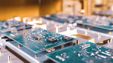
Modern PCB assembly operations achieve peak efficiency by integrating strategic component sourcing with advanced automation systems. Leading PCBA providers leverage robotic placement technologies to accelerate production cycles while maintaining sub-millimeter placement accuracy. A critical focus lies in balancing lean inventory practices with real-time supplier coordination, minimizing component shortages that disrupt high-volume PCB assembly workflows.
Predictive quality control frameworks, powered by machine vision and AI-driven defect detection, now reduce rework rates by up to 40% in complex PCB assemblies. Concurrently, modular production layouts enable rapid reconfiguration for mixed-batch orders without compromising throughput. These methodologies align with Industry 4.0 standards, creating synergies between automated PCB assembly lines and enterprise-level manufacturing execution systems (MES).
Forward-thinking PCBA manufacturers further optimize efficiency through thermal management innovations and dynamic traceability protocols, ensuring compliance across aerospace, medical, and IoT applications. This multilayered approach positions PCB assembly companies to meet evolving demands for precision, scalability, and traceability in electronics production ecosystems.
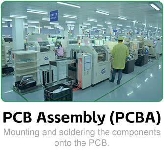
Automating PCB Assembly for Maximum Output
Modern PCB assembly workflows achieve peak productivity through strategic integration of robotic systems and AI-driven process optimization. By automating repetitive tasks like component placement and solder paste application, PCBA manufacturers reduce human error while scaling production capacity. High-speed pick-and-place robots equipped with machine vision now handle 85% of surface-mount device (SMD) installations, operating at rates exceeding 25,000 components per hour.
Tip: When implementing automation, prioritize systems with real-time thermal profiling to maintain solder joint integrity across varying production batches.
Advanced conveyor systems synchronize with automated optical inspection (AOI) stations, creating closed-loop feedback that adjusts assembly parameters mid-process. This approach reduces rework rates by 40% compared to manual quality checks. For mixed-technology boards combining SMD and through-hole components, dual-arm collaborative robots (cobots) enable seamless transitions between assembly stages without line stoppages.
The most efficient PCB assembly lines employ digital twin simulations to pre-validate workflows, identifying potential bottlenecks before physical production begins. By analyzing historical PCBA data, machine learning algorithms optimize material flow and equipment utilization rates, achieving takt time reductions of up to 22%. However, successful automation requires standardized component packaging and strict adherence to IPC-A-610 guidelines to ensure robotic systems operate at full potential.
Smart Component Sourcing for PCB Efficiency
Effective PCB assembly relies on strategic procurement practices that balance cost, availability, and quality. Leading PCBA providers optimize component sourcing by leveraging supplier partnerships and real-time market analytics to mitigate supply chain disruptions. For instance, dual-sourcing critical components like microcontrollers or capacitors ensures continuity, while automated inventory systems track consumption patterns to prevent overstocking or shortages.
| Sourcing Strategy | Key Benefit | Risk Mitigated |
|---|---|---|
| Supplier Diversification | Reduces dependency on single vendors | Geopolitical delays |
| Demand Forecasting | Aligns procurement with production cycles | Excess inventory costs |
| Component Substitution | Maintains flexibility in design | Obsolescence issues |
Advanced tools like AI-driven procurement platforms analyze historical data to predict price fluctuations, enabling proactive purchasing. Additionally, PCB assembly firms prioritize authenticity verification to combat counterfeit parts, employing X-ray inspection and batch tracing. By integrating these methods, manufacturers achieve shorter lead times and higher yield rates, directly supporting downstream processes like automated soldering and testing protocols. This systematic approach ensures seamless alignment with lean production goals while maintaining cost-efficiency.
Quality Control Tactics for PCB Assembly
Effective PCB assembly processes rely on rigorous quality control (QC) frameworks to ensure reliability in electronic devices. Leading PCBA providers implement multi-stage inspection protocols, combining automated optical inspection (AOI) with X-ray imaging to detect soldering defects, component misalignment, or micro-cracks invisible to the naked eye. Statistical process control (SPC) tools further enhance defect tracking by analyzing production data in real time, enabling immediate adjustments to soldering temperatures or placement accuracy.
To maintain consistency, advanced PCB assembly lines integrate inline testing modules that verify electrical functionality at critical stages. For instance, boundary scan testing identifies open circuits or shorted connections before final encapsulation, while environmental stress screening (ESS) exposes boards to thermal cycling and vibration to simulate long-term operational conditions. These tactics minimize field failures and align with ISO 9001 and IPC-A-610 standards, which define acceptability criteria for PCBA outputs.
Transitioning seamlessly from inspection to correction, automated defect classification systems categorize issues by severity, prioritizing rework for critical faults. This approach not only reduces waste but also supports continuous improvement initiatives—a bridge to lean methodologies discussed in subsequent sections. By embedding QC at every production node, manufacturers achieve first-pass yield rates exceeding 99%, cementing their role as partners in high-stakes electronics manufacturing.
Lean Methods in PCB Assembly Lines
Implementing lean manufacturing principles has become a cornerstone for PCB assembly companies aiming to eliminate waste and maximize productivity. By analyzing workflow patterns, value stream mapping identifies bottlenecks in PCBA processes, enabling manufacturers to reduce idle time between solder paste application, component placement, and reflow soldering. A key strategy involves adopting just-in-time (JIT) inventory systems, which synchronize material deliveries with production schedules to minimize storage costs and component obsolescence.
Standardized work instructions further enhance consistency across PCB assembly lines, ensuring operators follow optimized procedures for tasks like surface-mount technology (SMT) placement or through-hole soldering. Real-time data monitoring tools track cycle times and defect rates, allowing teams to implement rapid corrective actions when deviations occur. For instance, kaizen events—focused improvement workshops—often target solder joint quality or machine calibration accuracy, directly boosting yield rates.
When integrated with robotics in PCB assembly automation, lean methodologies create synergies that accelerate throughput without compromising precision. Cross-trained teams and modular workstation designs add flexibility, enabling PCBA providers to swiftly adapt to design changes or mixed-product batches. This systematic approach not only reduces non-value-added activities but also aligns with broader goals of efficient electronics production outlined in modern manufacturing frameworks.
Robotics in PCB Assembly Automation
Modern PCB assembly workflows increasingly rely on robotic systems to achieve unprecedented levels of speed and accuracy. Advanced PCBA lines now integrate collaborative robots (cobots) capable of handling delicate surface-mount devices (SMDs) with micron-level precision, reducing human error by up to 98% in component placement tasks. These systems utilize machine vision to verify part orientation and solder paste application in real time, ensuring compliance with IPC-A-610 standards.
The shift toward adaptive automation allows robots to dynamically adjust to varying board designs, enabling rapid product changeovers without compromising throughput. For instance, dual-arm robotic systems can simultaneously populate components on multiple PCB panels, cutting cycle times by 40–60% compared to manual processes. Furthermore, AI-driven predictive maintenance minimizes downtime by analyzing motor performance and wear patterns in robotic actuators.
By synchronizing robotics with PCB assembly line analytics, manufacturers achieve end-to-end traceability, tracking each board’s journey from component loading to final inspection. This integration not only accelerates production but also strengthens quality assurance—critical for industries requiring MIL-PRF-38534 compliance. As Industry 4.0 principles take root, the fusion of robotics and PCBA processes continues to redefine efficiency benchmarks in electronics manufacturing.
Efficient PCB Supply Chain Management
Effective PCB assembly operations rely on streamlined supply chain frameworks that synchronize material flow, vendor partnerships, and logistics. Leading PCBA providers implement real-time inventory tracking systems to mitigate delays, using IoT-enabled platforms to monitor component availability from certified suppliers. By adopting predictive analytics, manufacturers forecast demand fluctuations and align procurement cycles with production schedules, reducing excess stock while maintaining just-in-time delivery for critical parts.
Strategic supplier diversification further strengthens resilience, ensuring access to high-quality components even during global shortages. Automated procurement tools cross-reference bill of materials (BOM) data with supplier catalogs, minimizing human error in component sourcing. For PCB assembly workflows, consolidating shipments through regional hubs cuts lead times by 18–35%, while blockchain-based traceability solutions validate authenticity across multi-tiered supply networks.
Collaboration with PCBA partners extends to shared digital dashboards, enabling transparent communication on order status and potential bottlenecks. This integration ensures that design changes or urgent revisions propagate instantly through the supply chain, preventing costly rework. By balancing agility with cost-efficiency, manufacturers achieve continuous material flow—a critical factor in sustaining high-volume electronics production without compromising quality standards.
Precision PCB Assembly Best Practices
Achieving consistent precision in PCB assembly requires meticulous attention to both process design and execution. Leading PCBA providers begin with laser-focused component alignment, leveraging automated optical inspection (AOI) systems to verify placements within micron-level tolerances. This is complemented by precise solder paste application, where stencil thickness and aperture geometry are calibrated to match circuit board specifications, minimizing defects like bridging or insufficient joints.
To maintain accuracy, real-time process monitoring tools track variables such as reflow oven temperature profiles, ensuring adherence to manufacturer-recommended thermal curves. Advanced manufacturers also implement design for manufacturability (DFM) checks early in the prototyping phase, identifying potential alignment or spacing issues before full-scale production.
For high-density boards, microscopic inspection protocols become critical, particularly for ball grid array (BGA) components and fine-pitch ICs. Pairing robotic pick-and-place systems with AI-driven error detection reduces human intervention while enhancing repeatability. Additionally, traceability systems log each assembly step, enabling rapid root-cause analysis if deviations occur.
By integrating these practices, PCB assembly companies balance speed with precision, delivering robust electronic assemblies that meet stringent industry standards without compromising throughput. This approach not only aligns with lean manufacturing principles but also supports scalable solutions for complex PCBA projects.
Rigorous PCB Testing Protocols Guide
Modern PCB assembly processes rely on multilayered testing protocols to ensure reliability in mission-critical applications. Leading PCBA providers implement automated optical inspection (AOI) systems to detect soldering defects, component misalignment, and trace integrity issues at micron-level precision. Post-reflow, X-ray inspection validates hidden connections in ball grid array (BGA) components, while in-circuit testing (ICT) verifies electrical functionality against design specifications.
Notably, advanced PCB assembly workflows integrate environmental stress screening (ESS) to simulate thermal cycling and vibration exposure, identifying latent failures before deployment. To maintain traceability, serialized tracking systems document test results for each PCBA unit, enabling rapid root-cause analysis if anomalies emerge.
Transitioning from validation to continuous improvement, data-driven manufacturers correlate test outcomes with process parameters, refining solder paste application techniques and pick-and-place machine calibration. This closed-loop approach aligns with lean manufacturing principles discussed earlier, creating a cohesive quality ecosystem from component sourcing to final validation.
By enforcing tiered testing checkpoints—from pre-assembly material checks to post-production burn-in tests—PCB assembly companies mitigate risks while meeting time-to-market demands in high-volume electronics manufacturing.
Conclusion
As the electronics manufacturing landscape evolves, PCB assembly providers must balance technological innovation with operational discipline to maintain competitive advantage. Leading pcb assembly companies demonstrate that success hinges on integrating automated systems with human expertise, ensuring both speed and precision in PCBA processes. The strategic adoption of robotics and AI-driven inspection tools has redefined quality benchmarks, while data analytics now enable real-time adjustments in lean production workflows.
Equally critical is the synchronization of supply chain networks with just-in-time manufacturing principles, which minimizes component shortages and production delays. Forward-thinking firms are leveraging smart sourcing platforms to preemptively address material availability challenges, creating resilient ecosystems for high-mix PCB assembly. When combined with rigorous testing protocols, these approaches form a cohesive framework that drives continuous improvement across manufacturing cycles.
Ultimately, the convergence of advanced automation, supply chain intelligence, and zero-defect methodologies positions modern PCBA specialists to meet escalating demands for miniaturized, complex electronics without compromising reliability or turnaround times. This holistic operational philosophy will remain pivotal as industry standards for precision electronics manufacturing continue to rise.
FAQs
What distinguishes high-quality PCB assembly from basic prototyping?
PCB assembly becomes production-grade when manufacturers implement automated optical inspection (AOI) systems and adhere to IPC-A-610 standards. This ensures consistent solder joint quality and component alignment, critical for high-volume outputs.
How does supply chain optimization reduce lead times in PCBA?
Leading PCBA providers leverage vendor-managed inventory programs and real-time component tracking, minimizing delays caused by shortages. Multi-sourcing strategies for critical parts further mitigate risks in electronics manufacturing workflows.
Can robotic automation improve flexible PCB assembly precision?
Yes, 6-axis robotic arms with machine vision achieve ±25µm placement accuracy for miniature components like 0201 resistors. This reduces manual rework rates by up to 67% in mixed-technology assemblies combining SMT and through-hole parts.
What testing protocols ensure reliability in harsh-environment PCBAs?
Advanced PCB assembly lines employ in-circuit testing (ICT) combined with thermal cycling (-40°C to +125°C) to validate performance under stress. Functional testing with custom firmware simulates end-use conditions for mission-critical applications.
Why is traceability vital for medical-grade PCBA compliance?
ISO 13485-certified PCBA processes use laser-marked UID codes to track components from procurement to final assembly. This supports regulatory audits and enables rapid recalls if defects emerge post-production.
Optimize Your Production with Expert PCB Assembly Solutions
For tailored solutions that align with industry best practices, please click here to explore advanced PCBA capabilities designed for scalability and precision.