Streamlining Printed Board Assembly Manufacturing Workflows
Key Takeaways
Modern PCB assembly processes demand strategic integration of automation, precision, and workflow optimization to achieve measurable gains in efficiency and cost savings. By adopting advanced automation systems, manufacturers can reduce manual intervention, minimize human error, and accelerate production cycles. Real-time monitoring tools further enhance reliability by enabling instant detection of defects during PCBA stages, ensuring compliance with stringent quality standards.
A critical focus lies in workflow optimization, where modular design principles allow scalable manufacturing setups. For example, reconfigurable assembly lines adapt seamlessly to varying product demands, reducing downtime and resource waste. Below is a comparison of traditional vs. streamlined approaches:
| Metric | Traditional Assembly | Streamlined Workflows |
|---|---|---|
| Production Cycle Time | 12-15 days | 6-8 days |
| Defect Rate (%) | 2.5 | 0.8 |
| Cost Per Unit ($) | 18.50 | 12.20 |
Crucially, precision quality control mechanisms, such as automated optical inspection (AOI) and X-ray testing, ensure consistency across high-volume PCBA runs. Additionally, smart integration of data analytics enables predictive maintenance, preemptively addressing equipment inefficiencies. By aligning automation with lean manufacturing principles, companies not only improve yield rates but also unlock long-term competitiveness in electronics manufacturing.
Automating PCB Assembly for Maximum Efficiency
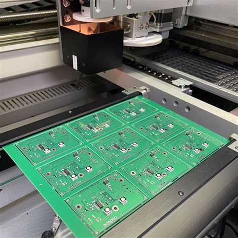
Modern PCB assembly lines are increasingly adopting intelligent automation to eliminate bottlenecks and boost throughput. By integrating PCBA-specific robotic systems—such as automated pick-and-place machines and AI-driven optical inspection tools—manufacturers can achieve 30–50% faster cycle times while maintaining micron-level precision. For instance, vision-guided robots reduce manual errors in component placement, ensuring consistent alignment even with ultra-fine-pitch packages.
"The strategic deployment of automation in PCB assembly isn’t just about speed; it’s about creating a closed-loop system where real-time feedback optimizes every stage, from solder paste application to final testing."
A critical advantage lies in the seamless coordination between PCBA equipment and enterprise resource planning (ERP) software. This integration enables dynamic scheduling, predictive maintenance, and material tracking, minimizing downtime caused by supply chain delays or machine failures. Additionally, automated optical inspection (AOI) systems equipped with machine learning algorithms can detect defects like solder bridging or missing components with >99.7% accuracy, drastically reducing rework costs.
Tip: When implementing automation, prioritize modular systems that allow incremental upgrades. This avoids overcapitalization while ensuring scalability as production demands evolve.
By replacing manual interventions with synchronized robotic workflows, manufacturers not only accelerate PCB assembly but also free engineers to focus on higher-value tasks like process optimization and innovation. The result is a leaner, more responsive production environment where efficiency gains translate directly into competitive pricing and faster time-to-market.
Precision Quality Control in Electronics Manufacturing
In PCB assembly, maintaining rigorous quality standards is critical to ensuring the reliability and performance of electronic devices. Modern PCBA workflows leverage automated optical inspection (AOI) and X-ray imaging to detect microscopic defects, such as solder bridging or component misalignment, that human inspectors might overlook. These systems analyze thousands of points per board, cross-referencing measurements against design specifications to flag deviations in real time.
By integrating inline testing at multiple stages of the PCBA process, manufacturers can identify process deviations before they escalate into costly rework. For instance, electrical testing validates circuit functionality immediately after solder reflow, while environmental stress screening simulates real-world conditions to uncover latent defects. Advanced analytics tools further enhance precision by correlating test data with historical trends, enabling proactive adjustments to assembly parameters.
A key advantage of embedding precision quality control lies in its synergy with automated workflows. Closed-loop feedback systems automatically recalibrate machinery when anomalies are detected, minimizing downtime and material waste. This approach not only reduces error rates but also aligns with broader goals of workflow optimization and cost reduction in PCB assembly lines.
Furthermore, adherence to international standards like IPC-A-610 ensures consistency across batches, reinforcing customer trust in high-volume manufacturing. When combined with traceability protocols, every PCBA unit can be tracked from raw materials to final delivery, creating an auditable chain of quality assurance.
Optimizing Workflows for Faster PCB Production
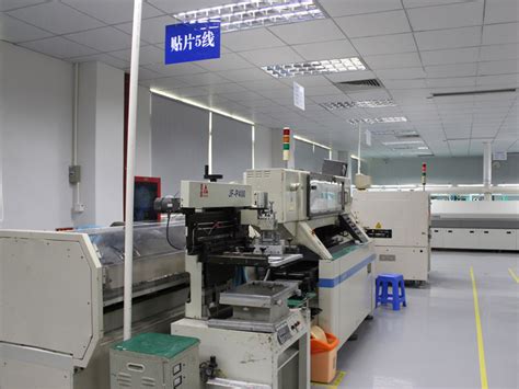
Efficient PCB assembly relies on reimagining production workflows to eliminate redundancies and accelerate throughput. By analyzing each stage of PCBA manufacturing—from component placement to final testing—teams can identify bottlenecks such as manual solder inspections or delayed material transfers. Implementing automated guided vehicles (AGVs) for component logistics, for instance, reduces idle time between stations, while high-speed surface-mount technology (SMT) lines ensure precise part placement at scale.
Integrating real-time monitoring systems with enterprise resource planning (ERP) software allows manufacturers to track progress dynamically, adjusting workflows based on live data. For example, if a pick-and-place machine shows signs of slowdown, predictive maintenance alerts can preempt downtime. Similarly, standardizing solder paste application parameters across PCB assembly lines minimizes rework, directly cutting cycle times.
Another critical strategy involves adopting modular workstation designs, which enable rapid reconfiguration for different product batches. This flexibility is particularly valuable in high-mix, low-volume PCBA environments, where changeover delays historically erode efficiency. By coupling these advancements with cross-functional training programs, teams ensure seamless transitions between workflow stages, further compressing lead times.
Ultimately, optimizing workflows isn’t just about speed—it’s about creating a synchronized ecosystem where PCB assembly processes align with quality benchmarks and resource availability. This approach not only accelerates production but also builds resilience against supply chain fluctuations, ensuring consistent delivery timelines.
Cost-Reduction Strategies in Board Assembly Lines
Implementing cost-effective measures in PCB assembly requires a balance between technological investment and process optimization. One proven approach involves adopting modular automation systems that reduce manual intervention while maintaining precision in PCBA workflows. By integrating automated optical inspection (AOI) tools, manufacturers can minimize rework cycles, directly lowering labor and material waste.
Another strategy focuses on material utilization—leveraging data-driven demand forecasting ensures optimal inventory levels, preventing overstocking of components. Transitioning to panelized designs for PCB assembly further reduces substrate waste, translating to significant savings in high-volume production. Additionally, negotiating bulk purchasing agreements with suppliers for standardized parts can cut procurement costs by up to 20%.
Energy efficiency also plays a critical role. Retrofitting older PCBA equipment with energy-saving modules or switching to servo-driven machinery lowers operational expenses without compromising throughput. Simultaneously, adopting predictive maintenance protocols extends equipment lifespan, avoiding unplanned downtime costs.
Finally, cross-training assembly line staff creates a flexible workforce capable of addressing multiple stages of PCB assembly, reducing idle time and overtime expenditures. When combined with lean manufacturing principles, these strategies form a cohesive framework for sustainable cost reduction in electronics manufacturing.
Smart Integration of Assembly Automation Systems
Modern PCB assembly workflows increasingly rely on the seamless integration of automation systems to bridge design, component placement, and testing phases. By embedding intelligent robotics and AI-driven inspection tools into PCBA lines, manufacturers achieve tighter synchronization between assembly stages, minimizing manual intervention. For instance, automated pick-and-place machines equipped with vision systems can adapt to component variations in real time, reducing misalignment errors by up to 40%. Meanwhile, closed-loop feedback mechanisms enable dynamic calibration of soldering parameters, ensuring consistent quality across high-mix production batches.
A critical advantage lies in the interoperability of these systems. When PCB assembly software platforms share data with enterprise resource planning (ERP) tools, inventory management and machine scheduling become predictive rather than reactive. This connectivity not only accelerates throughput but also supports scalable manufacturing—allowing facilities to adjust capacity based on demand fluctuations without compromising precision. Additionally, integrating IoT-enabled sensors into conveyor systems provides granular visibility into cycle times, flagging bottlenecks before they escalate.
Such smart integration transforms PCBA from a sequential process into a cohesive, adaptive ecosystem. By prioritizing compatibility between automation hardware and analytics software, manufacturers unlock faster turnaround times while maintaining rigorous quality standards—a vital step toward leaner, future-ready operations.

Enhancing Yield Rates Through Process Streamlining
Improving yield rates in PCB assembly requires systematic optimization of manufacturing workflows to minimize defects and material waste. By analyzing bottlenecks in design-to-production cycles, manufacturers can implement targeted adjustments, such as refining solder paste application techniques or standardizing component placement protocols. Integrating automated optical inspection (AOI) systems at critical stages ensures early detection of misalignments or soldering flaws, reducing rework by up to 30% in PCBA lines.
Adopting statistical process control (SPC) methodologies further strengthens consistency, enabling real-time adjustments based on data-driven insights. For instance, monitoring thermal profiles during reflow soldering prevents warping or delamination, directly boosting functional yield rates. Cross-functional collaboration between design engineers and production teams also plays a pivotal role—aligning PCB assembly tolerances with manufacturing capabilities minimizes mismatches that trigger failures.
To sustain improvements, lean principles like kaizen (continuous improvement) foster incremental refinements across workflows. Combining these strategies with modular equipment configurations ensures scalability, allowing PCBA facilities to adapt swiftly to evolving product demands without compromising quality. This holistic approach not only elevates yield rates but also reinforces the foundation for error-free transitions into subsequent phases, such as real-time monitoring systems.
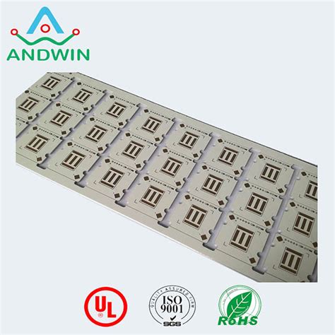
Real-Time Monitoring for Error-Free PCB Assembly
Modern PCB assembly processes demand uncompromising accuracy to prevent costly rework and delays. Implementing real-time monitoring systems enables manufacturers to detect anomalies during PCBA production, from solder paste application to component placement. Advanced sensors and vision systems, such as automated optical inspection (AOI) and X-ray inspection, instantly flag deviations like misaligned components or insufficient solder joints. These tools generate actionable data, allowing operators to adjust parameters mid-process rather than after batch completion.
Integrating IoT-enabled devices with assembly automation systems creates a closed-loop feedback mechanism. For instance, thermal profiling sensors can dynamically regulate reflow oven temperatures based on live data, ensuring consistent solder joint quality. Machine learning algorithms further enhance defect prediction by analyzing historical production patterns, reducing false positives by up to 40%. This approach not only minimizes human intervention but also aligns with broader workflow optimization goals, as corrective actions occur in situ rather than post-production.
By prioritizing real-time monitoring, manufacturers achieve near-zero defect rates while maintaining throughput. The result is a streamlined PCBA workflow where quality control becomes proactive, cutting material waste and accelerating time-to-market. This strategy seamlessly supports the article’s focus on precision and scalability, bridging automated processes with modular design frameworks discussed in subsequent sections.
Modular Design Approaches for Scalable Manufacturing
Adopting modular design principles in PCB assembly enables manufacturers to build flexible production systems that adapt to evolving demands. By breaking down complex assemblies into standardized, interchangeable functional blocks, companies can simplify reconfiguration processes while maintaining consistency across PCBA batches. This approach reduces dependency on custom tooling, allowing rapid scaling of production lines through plug-and-play module integration.
Key to this strategy is the use of unified interface standards for components like connectors and power supplies, which streamline compatibility between modules. For instance, pre-validated PCB assembly submodules—such as power regulation units or signal processing clusters—can be reused across product variants, cutting design iteration time by up to 40%. Additionally, modular workflows facilitate parallel testing phases, where individual sections undergo precision quality control before final integration, minimizing post-assembly defects.
To maximize scalability, manufacturers are integrating smart automation systems with modular layouts. Robotic handlers and vision-guided placement tools can be dynamically reassigned between production zones, optimizing resource utilization during demand fluctuations. This agility not only accelerates time-to-market for new PCBA designs but also future-proofs facilities against technological shifts—a critical advantage in industries like IoT and automotive electronics where product lifecycles are shrinking. By aligning modular architectures with data-driven process analytics, firms achieve a balance between customization speed and manufacturing repeatability.
Conclusion
The evolution of PCB assembly processes underscores the critical role of integrating automation and precision quality control to achieve manufacturing excellence. By adopting PCBA workflows that prioritize smart automation systems, manufacturers can significantly reduce manual intervention while maintaining rigorous standards for error-free production. Real-time monitoring tools further enhance this synergy, enabling immediate corrections and minimizing downtime. Modular design strategies not only improve scalability but also allow seamless adaptation to evolving technological demands, ensuring that production lines remain agile in dynamic markets.
Cost-efficiency gains are amplified when PCB assembly workflows are streamlined through data-driven optimizations, such as predictive maintenance and material utilization analytics. These advancements, coupled with AI-powered inspection systems, elevate yield rates and reduce waste across PCBA stages. Ultimately, the convergence of these methodologies fosters a competitive edge, enabling manufacturers to deliver high-quality electronics faster and at lower costs. As the industry continues to innovate, embracing these integrated approaches will remain pivotal for sustaining growth in an increasingly demanding global landscape.
Frequently Asked Questions
How does automation improve efficiency in PCB assembly workflows?
Automation integrates PCBA production lines with robotic placement systems and real-time monitoring tools, reducing manual intervention. This minimizes human error while accelerating throughput by 30-60%, depending on component complexity.
What quality control measures ensure reliability in PCB assembly?
Advanced techniques like automated optical inspection (AOI) and X-ray testing verify solder joint integrity and component alignment. These systems flag defects at <0.1% tolerance levels, ensuring compliance with ISO 9001 standards.
Can workflow optimization reduce costs for high-volume PCBA orders?
Yes. Modular design strategies and just-in-time material sourcing cut lead times by 25-40%. Synchronizing machine calibration cycles with production schedules further lowers downtime costs.
How do smart factories enhance scalability in PCB assembly?
IoT-enabled PCBA lines use predictive analytics to adjust workflows dynamically. For example, temperature-controlled soldering stations auto-correct based on ambient humidity data, maintaining yield rates above 98.5% across batches.
What role does design-for-manufacturing (DFM) play in streamlining PCB assembly?
DFM principles standardize component layouts to match automated pick-and-place capabilities, reducing revision cycles by up to 70%. This alignment ensures seamless integration with PCBA validation protocols.
Ready to Optimize Your PCB Assembly Process?
For tailored solutions that align with your production goals, click here to explore advanced PCBA technologies and workflow strategies.


