Through Hole Assembly Optimization for Reliable PCB Designs
Key Takeaways
Effective PCB assembly relies on strategic planning across multiple design phases. Proper component placement directly impacts thermal performance and signal integrity, particularly in through hole assembly where mechanical stability is critical. Prioritize thermal management by spacing heat-sensitive components away from high-power elements and incorporating adequate copper relief in plated through holes. Compliance with IPC standards ensures consistent solder joint quality, minimizing voids and cold joints during PCBA manufacturing.
Durability hinges on selecting appropriate solder alloys and validating hole-to-lead ratios to withstand mechanical stress. For signal integrity, maintain controlled impedance by optimizing trace routing and avoiding parallel runs near through holes. PCB layout strategies, such as grouping analog and digital components separately, reduce electromagnetic interference. Finally, iterative prototyping and testing validate design choices, ensuring through hole assembly meets both functional and longevity requirements.
Thermal Management in PCB Assembly
Effective thermal management forms the backbone of reliable PCB assembly processes, particularly in through hole designs where component density and power dissipation create unique challenges. Proper heat distribution begins with strategic component placement—positioning high-power devices away from thermally sensitive parts while leveraging thermal vias or copper pours to channel heat toward outer layers. During PCBA manufacturing, soldering techniques like wave soldering must account for thermal expansion coefficients to prevent joint stress, especially in multilayer boards.
Adherence to IPC-2221 standards ensures adequate clearance between heat-generating components and adjacent traces, minimizing thermal interference that could degrade signal integrity. Engineers often integrate heatsinks or thermally conductive adhesives in through hole assembly to enhance heat dissipation, particularly in industrial or automotive applications. Real-time thermal profiling during reflow cycles further optimizes temperature gradients, reducing the risk of delamination or solder cracks. By balancing material selection, layout design, and process controls, robust thermal management in PCB assembly directly correlates with long-term durability and performance stability.

IPC Compliance in Through Hole Assembly
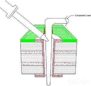
Adhering to IPC standards ensures consistent quality and reliability in through hole assembly processes for PCB assembly (PCBA). These guidelines address critical factors such as component lead protrusion, solder fillet formation, and hole wall integrity. For instance, IPC-A-610 specifies acceptable solder joint criteria, while IPC-6012 defines performance requirements for rigid circuit boards.
"Compliance with IPC standards reduces manufacturing defects by up to 70%, according to industry studies. Always validate hole-to-lead diameter ratios and annular ring widths during design reviews."
In through hole assembly, maintaining proper thermal relief patterns and avoiding pad lifting during soldering are essential for durability. Automated inspection tools, like automated optical inspection (AOI), help verify compliance with IPC Class 2 or Class 3 requirements, depending on the application’s criticality. For high-reliability PCBA projects, ensure plating thickness meets IPC-2221 specifications to prevent barrel cracking under thermal stress.
Transitioning from design to production requires cross-functional collaboration. Engineers must align PCB assembly parameters—such as wave soldering temperatures—with IPC J-STD-001 guidelines to achieve uniform solder penetration without damaging heat-sensitive components. Regularly auditing supplier processes against these standards further mitigates risks in complex assemblies.
Signal Integrity in Through Hole Design
Maintaining signal integrity in through hole assembly requires careful consideration of component placement, trace routing, and impedance control. Unlike surface-mount components, through-hole parts introduce unique challenges due to their vertical connections, which can create unintended inductive loops or capacitive coupling. To mitigate these effects, designers should prioritize PCB layout strategies such as minimizing trace lengths between vias and ensuring proper grounding for high-frequency signals.
In PCBA processes, the choice of through-hole plating material significantly impacts signal performance. For instance, copper-filled vias with controlled impedance reduce signal attenuation, especially in multi-layer boards. Compliance with IPC standards for hole diameter and annular ring width ensures consistent solder joints, which are critical for minimizing electrical noise. Additionally, staggered via placement and the use of ground planes between signal layers help isolate sensitive traces from interference.
Thermal management also plays a role in preserving signal integrity. Excessive heat during PCB assembly can warp substrates or degrade dielectric materials, altering impedance characteristics. By integrating thermal relief pads and optimizing solder wave profiles, manufacturers balance heat distribution without compromising electrical performance. These practices, when aligned with rigorous testing protocols like time-domain reflectometry, ensure reliable signal transmission in complex through-hole designs.
Durable PCB Soldering Techniques
Achieving reliable solder joints in PCB assembly requires precise control over materials, processes, and environmental factors. For through hole components, proper wetting of solder to both the pin and plated hole is critical to ensure mechanical stability and electrical conductivity. Using a lead-free solder alloy (e.g., SAC305) with a suitable melting profile helps balance durability and compliance with environmental regulations.
In PCBA workflows, wave soldering remains a common method for through hole connections, but optimizing parameters like conveyor speed, preheat temperature, and solder wave height is essential to prevent defects such as cold joints or tombstoning. For manual repairs, maintaining a consistent iron tip temperature (typically 300–350°C) and using flux-core solder wire minimize thermal stress on components.
Adherence to IPC-A-610 standards for solder fillet geometry ensures joints meet industry benchmarks for strength and longevity. Additionally, post-soldering inspections—including automated optical inspection (AOI) or X-ray analysis—help identify microcracks or voids that could compromise reliability. Integrating these practices with robust thermal management strategies (e.g., heat sinks near high-power components) further mitigates long-term degradation risks in demanding environments.
By aligning soldering techniques with material science and process controls, manufacturers can enhance the durability of through hole assemblies while maintaining signal integrity across the board.
Through Hole Assembly Durability Tips
Achieving durable through hole assembly in PCB assembly requires attention to mechanical stability and environmental resilience. Start by ensuring proper lead protrusion and solder fill ratios, as insufficient solder joints or excessive trimming can compromise structural integrity. Thermal cycling resistance is enhanced when using conformal coatings to protect against moisture and contaminants, particularly in harsh operating environments.
Adherence to IPC-A-610 standards for hole wall wetting and fillet formation minimizes void formation, a common failure point in PCBA applications. For high-vibration scenarios, reinforce connections with epoxy staking or anchor tabs to prevent component loosening over time. Additionally, selecting high-Tg substrates (e.g., FR-4 with Tg >170°C) improves thermal endurance, reducing board warping during repeated heating cycles.
Another key element is optimizing plated through hole (PTH) aspect ratios. Ratios exceeding 8:1 increase the risk of incomplete plating, weakening via durability. Pair this with lead-free solder alloys (e.g., SAC305) to meet RoHS compliance while maintaining joint reliability. Finally, implement automated optical inspection (AOI) during PCBA testing to identify micro-cracks or insufficient solder coverage before deployment. Combining these practices ensures through hole assemblies withstand mechanical stress and environmental challenges, aligning with long-term reliability goals.
PCB Layout for Efficient Through Holes
Effective PCB assembly relies on strategic layout planning to optimize through hole functionality while maintaining signal integrity and manufacturability. Designers should prioritize component grouping based on signal flow and power requirements, ensuring minimal trace lengths between through hole pins and adjacent surface-mount devices. A 0.1–0.3 mm annular ring width is recommended for plated holes to balance solder adhesion and mechanical stability during PCBA processes.
Critical considerations include:
- Drill-to-copper clearance: Maintain ≥0.15 mm to prevent solder bridging
- Thermal relief patterns for ground/power planes (4–6 spokes, 0.2 mm width)
- Symmetrical pad sizing for multi-pin connectors to avoid tombstoning
| Design Parameter | Recommended Specification | Impact on Assembly |
|---|---|---|
| Hole diameter tolerance | ±0.05 mm | Prevents misalignment |
| Pad-to-hole ratio | 1.8:1 | Reduces solder voids |
| Adjacent hole spacing | 2× hole diameter | Minimizes thermal stress |
For mixed-technology boards (through hole and SMD), stagger component orientations to streamline wave soldering. Implement teardrop-shaped pad transitions where traces meet holes, enhancing mechanical strength and reducing fracture risks. These practices not only improve PCBA yield rates but also align with IPC-2221 standards for long-term reliability. Transitioning to optimized layouts requires balancing design constraints with manufacturing realities—a crucial step in achieving robust through hole assembly outcomes.
Optimizing PCB Component Placement
Effective PCB assembly begins with strategic component placement, which directly impacts manufacturability and long-term reliability. When arranging through-hole components, thermal gradients and signal pathways must be prioritized to avoid interference. Group parts by function—such as power regulation or analog circuits—to minimize trace lengths and reduce electromagnetic noise. Maintain adequate spacing between heat-generating components (e.g., resistors, transformers) and temperature-sensitive devices to simplify PCBA soldering processes and prevent thermal stress.
For high-density layouts, align polarized components uniformly to streamline insertion during automated assembly. Place taller parts, such as electrolytic capacitors, away from board edges to avoid mechanical damage during handling. Additionally, position connectors and test points for accessibility, ensuring compliance with IPC standards for inspection and rework. Designers should also consider current-carrying capacity when routing traces to vias, as improper sizing can lead to voltage drops or overheating.
Transitioning to soldering, ensure pad sizes match lead diameters to achieve robust solder fillets. This alignment not only enhances through hole assembly durability but also supports consistent signal integrity by reducing parasitic inductance. By balancing spatial efficiency with thermal and electrical requirements, engineers can optimize both performance and longevity in PCBA designs.
Conclusion
Effective through hole assembly optimization culminates in balancing precision, compliance, and functional resilience. By prioritizing strategic component placement and adhering to IPC-610 standards, designers ensure robust PCB assembly workflows that minimize mechanical stress and signal degradation. Incorporating advanced soldering techniques, such as wave soldering or selective coating, enhances joint durability while mitigating thermal fatigue—a critical factor for high-reliability PCBA applications.
Thermal management remains equally critical, particularly in multilayer designs where heat dissipation directly impacts long-term performance. Aligning pad sizes, hole diameters, and annular ring specifications with IPC compliance reduces risks of solder voids or cracking. Additionally, maintaining signal integrity demands meticulous attention to trace routing and grounding strategies, especially in mixed-technology boards combining through hole and surface-mount components.
Ultimately, a holistic approach to through hole assembly—integrating design foresight, process rigor, and validation testing—ensures durable and high-performing PCBs. By leveraging these principles, engineers can achieve repeatable success in PCBA projects, meeting both functional demands and industry reliability benchmarks.
FAQs
How does component placement affect through hole assembly reliability?
Proper component placement minimizes signal path lengths and reduces thermal stress. In PCB assembly, positioning heat-sensitive parts away from high-power components ensures better thermal management and long-term durability.
What soldering techniques enhance through hole durability?
Wave soldering remains the standard for PCBA, but selective soldering improves precision for dense layouts. Ensuring adequate solder fillets and avoiding tombstoning are critical for mechanical stability under vibration or thermal cycling.
Why is IPC-A-610 compliance crucial for PCB assembly?
Adhering to IPC standards guarantees consistent solder joint quality, hole fill rates, and lead protrusion limits. This compliance reduces defects like cold joints or insufficient wetting, directly impacting signal integrity and product lifespan.
Can through hole designs coexist with surface-mount technology (SMT)?
Yes, mixed-technology PCBA is common. However, prioritize component spacing to prevent solder bridging, and use thermal relief pads to balance heat distribution during reflow processes.
How does board layout influence through hole performance?
Optimizing trace widths and avoiding sharp angles near holes minimizes impedance discontinuities. Separating high-speed and analog traces reduces crosstalk, preserving signal integrity in complex designs.
Optimize Your Next PCB Assembly Project
Ready to implement these best practices? Click here to consult with our experts for tailored PCBA solutions that prioritize reliability and efficiency.