Mastering PCB Design with Eagle CAD: A Comprehensive Guide
Introduction
Printed Circuit Board (PCB) design is a critical aspect of electronic product development. Engineers and hobbyists rely on powerful software tools to create efficient and reliable PCB layouts. Among the most popular PCB design tools is Eagle CAD (Easily Applicable Graphical Layout Editor), developed by Autodesk. Eagle CAD provides a robust platform for schematic capture, PCB layout, and autorouting, making it a preferred choice for both beginners and professionals.
This article explores Eagle CAD’s key features, workflow, best practices, and advanced techniques to help designers master PCB design efficiently.
1. Understanding Eagle CAD
1.1 Overview
Eagle CAD is a widely used electronic design automation (EDA) tool that supports schematic design and PCB layout. It offers a user-friendly interface, extensive component libraries, and powerful design rule checking (DRC) capabilities. Eagle is available in multiple versions, including:
- Free Version: Limited to two schematic sheets and two signal layers.
- Standard & Premium Versions: Support larger designs and additional features.
1.2 Key Features
- Schematic Editor: Allows designers to create circuit diagrams with ease.
- PCB Layout Editor: Provides tools for component placement and trace routing.
- Autorouter: Automates trace routing to save time.
- Design Rule Check (DRC): Ensures manufacturability by validating PCB constraints.
- Library Editor: Enables customization of components and footprints.
- 3D Visualization: Allows viewing the PCB in a three-dimensional space.
- ULP (User Language Programs): Extends functionality through custom scripts.
2. Eagle CAD Workflow
Designing a PCB in Eagle CAD follows a structured workflow:
2.1 Schematic Design
- Create a New Project: Start by setting up a project in Eagle’s Control Panel.
- Add Components: Use Eagle’s built-in libraries or create custom parts.
- Draw Connections: Place wires and nets to define electrical connections.
- Annotate and ERC: Assign reference designators and run an Electrical Rule Check (ERC) to detect errors.
2.2 PCB Layout
- Generate Board from Schematic: Switch to the board editor to begin layout.
- Component Placement: Arrange components logically for optimal routing.
- Manual and Autorouting: Route traces manually or use the autorouter.
- Design Rule Check (DRC): Verify trace widths, clearances, and other constraints.
- Silkscreen and Documentation: Add labels, logos, and manufacturing notes.
2.3 Exporting for Manufacturing
- Gerber Files: Generate industry-standard Gerber files for fabrication.
- Bill of Materials (BOM): Export a component list for procurement.
- 3D Models: Export STEP files for mechanical integration.
3. Best Practices for Efficient PCB Design
3.1 Schematic Design Tips
- Use Hierarchical Sheets: Break large designs into manageable sections.
- Label Nets Clearly: Improves readability and debugging.
- Avoid Floating Pins: Ensure all connections are properly terminated.
3.2 PCB Layout Optimization
- Component Placement:
- Group related components (e.g., power supply, MCU, connectors).
- Minimize trace lengths to reduce signal interference.
- Routing Strategies:
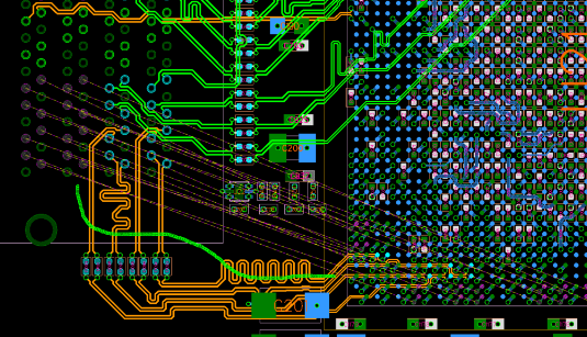
- Use 45° or curved traces instead of 90° angles to avoid EMI issues.
- Prioritize power and ground traces to ensure stable voltage distribution.
- Ground Planes:
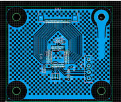
- Implement a solid ground plane to reduce noise and improve signal integrity.
- Thermal Management:
- Add thermal reliefs for soldering ease.
- Use copper pours for heat dissipation.
3.3 Design Rule Check (DRC) Settings
- Trace Width: Adjust based on current requirements (e.g., 10 mil for signals, 20+ mil for power).
- Clearance: Ensure sufficient spacing between traces to prevent short circuits.
- Via Sizing: Use appropriate via diameters for current-carrying capacity.
4. Advanced Techniques in Eagle CAD
4.1 Custom Library Creation
Eagle allows users to create custom components when existing libraries are insufficient.
- Open the Library Editor.
- Define the schematic symbol and PCB footprint.
- Map symbol pins to footprint pads.
- Save the component for reuse.
4.2 Autorouter Optimization
While manual routing offers better control, the autorouter can save time:
- Adjust Routing Grid and Topology Settings.
- Define Routing Priority (e.g., power traces first).
- Use Ripup & Retry for iterative improvements.
4.3 Scripting with ULPs
Eagle supports User Language Programs (ULPs) for automation:
- Generate custom reports (e.g., BOM, netlist).
- Automate repetitive tasks (e.g., renaming components).
- Export data in different formats.
4.4 3D Visualization
Eagle integrates with Autodesk Fusion 360 for 3D PCB modeling:
- Export the board as a STEP file.
- Visualize mechanical fit within enclosures.
- Detect potential collisions with other components.
5. Common Challenges & Solutions
5.1 Footprint Mismatches
- Problem: Incorrect footprints lead to assembly issues.
- Solution: Double-check datasheets and use verified libraries.
5.2 Signal Integrity Issues
- Problem: High-speed signals suffer from crosstalk.
- Solution: Use differential pairs, impedance matching, and ground shielding.
5.3 Manufacturing Errors
- Problem: Gerber files have missing layers or incorrect dimensions.
- Solution: Run DRC and verify Gerber output with a viewer like Gerbv.
6. Conclusion
Eagle CAD remains a powerful and accessible tool for PCB design, catering to hobbyists and professionals alike. By mastering schematic design, PCB layout, and advanced features like ULPs and 3D modeling, designers can create high-quality, manufacturable boards efficiently. Following best practices—such as proper component placement, optimized routing, and thorough DRC checks—ensures reliable and cost-effective PCB production.
As technology evolves, Eagle CAD continues to integrate new features, making it an indispensable tool in the electronics design ecosystem. Whether you’re designing a simple Arduino shield or a complex multi-layer PCB, Eagle CAD provides the tools needed to bring your ideas to life.
Further Learning Resources
- Official Eagle CAD Tutorials: Autodesk Eagle Learning
- YouTube Channels: Contextual Electronics, Phil’s Lab
- Books: “PCB Design Using Autodesk Eagle” by Matthew Scarpino
By investing time in learning Eagle CAD’s capabilities, designers can significantly enhance their PCB development workflow and produce professional-grade circuit boards.

