The Evolution and Impact of PCB Live Cam Technology in Modern Electronics
Introduction to PCB Live Cam Systems
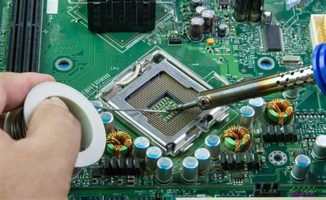
Printed Circuit Board (PCB) live camera systems, commonly referred to as PCB live cams, have revolutionized quality control, manufacturing processes, and educational demonstrations in the electronics industry. These specialized camera systems provide real-time visualization of PCB assembly, inspection, and testing procedures, offering unprecedented visibility into processes that were traditionally opaque to all but the technicians directly handling the boards.
PCB live cam technology integrates high-resolution imaging systems with advanced software analytics to monitor every aspect of PCB production and testing. From automated optical inspection (AOI) to live demonstrations of circuit functionality, these systems have become indispensable tools in modern electronics manufacturing facilities, research laboratories, and educational institutions.
Technical Components of PCB Live Cam Systems
A complete PCB live cam setup consists of several critical components working in harmony:
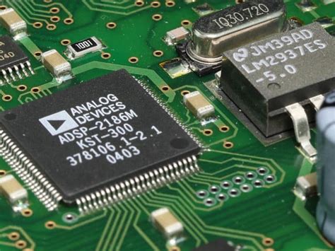
- High-Resolution Imaging Module: Modern systems use 4K or even 8K resolution cameras with macro lenses capable of capturing minute details down to 01005 package components (0.4mm × 0.2mm). Advanced systems incorporate multiple cameras for top-down, oblique, and side-view perspectives.
- Lighting Systems: Specialized LED illumination with adjustable color temperatures (typically 3000K-6500K) and multi-directional lighting setups eliminate shadows and provide optimal contrast for component inspection. Some systems incorporate coaxial lighting for better reflection control.
- Precision Positioning: Motorized XYZ stages with micron-level precision allow for accurate positioning and scanning of entire PCB panels. High-end systems may include rotational axes for angled viewing.
- Real-Time Processing Hardware: FPGA or GPU-accelerated image processing enables immediate analysis of captured images without lag. This is particularly critical for inline inspection systems.
- Software Suite: Comprehensive software packages handle image acquisition, processing, analysis, and integration with manufacturing execution systems (MES). Advanced features include component recognition, solder joint analysis, and comparison against golden samples.
Applications in Manufacturing and Quality Control
Automated Optical Inspection (AOI)
PCB live cams form the core of modern AOI systems, scanning boards at production speeds while identifying:
- Component placement errors (missing, misaligned, or wrong components)
- Solder defects (bridges, insufficient solder, cold joints)
- Polarity and orientation mistakes
- Physical damage or contamination
Modern systems can inspect up to 20,000 components per hour with defect detection rates exceeding 99.9%, far surpassing human capabilities in both speed and accuracy.
Solder Paste Inspection (SPI)
Prior to component placement, PCB live cams with 3D imaging capabilities measure:
- Solder paste volume and height distribution
- Pad coverage percentage
- Bridge risk assessment
- Stencil cleaning effectiveness
This preventive inspection catches potential defects before they propagate through the assembly process, significantly reducing rework costs.
Conformal Coating Inspection
For boards requiring protective coatings, live cam systems verify:
- Coating thickness uniformity
- Coverage completeness (especially around tall components)
- Absence of bubbles or contaminants
- Proper masking of excluded areas
Live Demonstration and Educational Applications
Beyond manufacturing, PCB live cams have transformed how electronics are demonstrated and taught:
Real-Time Circuit Visualization
Educational institutions and trade shows use live cam setups to demonstrate:
- Signal propagation through circuits
- Thermal behavior under load (when paired with thermal imaging)
- Component-level operation (showing individual ICs, transistors, or passive components in action)
- Failure modes and debugging processes
Remote Collaboration and Support
High-quality PCB live streams enable:
- Remote technical support with experts guiding repairs via live video
- Collaborative design reviews with distributed teams
- Virtual inspections for quality assurance across global supply chains
- Live training sessions without physical proximity constraints
Advanced Features in Modern PCB Live Cam Systems
AI-Powered Defect Recognition
Machine learning algorithms trained on millions of defect examples can now:
- Identify novel defect patterns not explicitly programmed
- Continuously improve detection accuracy through operation
- Reduce false positives by understanding acceptable process variations
- Predict potential future failures based on subtle early indicators
Augmented Reality Overlays
Advanced systems superimpose:
- Component identifiers and specifications
- Expected vs. actual values at test points
- Schematic representations over physical layouts
- Rework instructions directly on defect locations
High-Speed Imaging
Specialized cameras capturing thousands of frames per second allow analysis of:
- Wave soldering dynamics
- Mechanical stress testing
- Vibration-induced failures
- Transient electrical phenomena
Integration with Industry 4.0 Systems
Modern PCB live cams don’t operate in isolation but connect to broader smart manufacturing ecosystems:
- MES Integration: Inspection results automatically update manufacturing execution systems, triggering process adjustments or maintenance alerts.
- Predictive Maintenance: Camera data combined with equipment telemetry predicts when cleaning or calibration is needed before defects occur.
- Digital Twin Synchronization: Live images continuously update digital representations of physical boards for complete traceability.
- Blockchain Verification: Image hashes stored on blockchain provide immutable quality records for high-reliability applications.
Technical Challenges and Solutions
Despite their advantages, PCB live cam systems face several technical challenges:
- Resolution vs. Speed Tradeoff: Higher resolutions reduce processing speed. Solutions include:
- Region-of-interest processing (only analyzing changed areas)
- Multi-camera parallel processing
- Smart compression algorithms
- Reflective Surface Handling: Components with shiny surfaces create imaging artifacts. Advanced systems combat this with:
- Multi-angle lighting and imaging
- Polarization filters
- Computational imaging techniques
- 3D Component Obstruction: Tall components shadow nearby areas. Solutions involve:
- Oblique angle cameras
- Laser triangulation systems
- Photometric stereo techniques
- Environmental Variations: Temperature fluctuations and vibrations affect measurements. Modern systems incorporate:
- Active temperature stabilization
- Vibration isolation platforms
- Reference object calibration
Future Developments in PCB Live Cam Technology
Emerging trends point toward several exciting developments:
- Hyperspectral Imaging: Going beyond visible light to analyze material composition and contamination through spectral signatures.
- Quantum Imaging Sensors: Utilizing quantum properties of light for unprecedented sensitivity in low-light conditions.
- Holographic Inspection: Full 3D volumetric imaging of boards and components for complete internal and external inspection.
- Edge AI Processing: Moving more analysis directly to camera modules for reduced latency and bandwidth requirements.
- Autonomous Rework Integration: Systems that not only identify defects but automatically initiate and guide repair processes.
Conclusion
PCB live cam technology has evolved from simple inspection tools to comprehensive process monitoring and analysis systems that form the backbone of modern electronics manufacturing. As resolution, speed, and intelligence continue to improve, these systems will play an even greater role in ensuring product quality, enabling remote collaboration, and advancing electronics education. The integration of AI, advanced imaging techniques, and Industry 4.0 connectivity promises to further enhance their capabilities, making PCB live cams indispensable in the increasingly complex world of electronic device manufacturing and maintenance.
From enabling near-perfect production quality to democratizing access to electronic manufacturing knowledge, PCB live camera systems represent a perfect marriage of optical technology and electronic engineering that will continue to drive innovation in both fields for years to come.