Streamlining PCBA Printed Circuit Board Manufacturing Processes
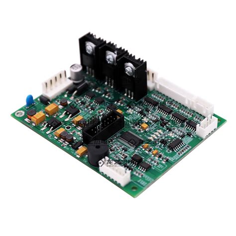
Key Takeaways
Effective PCBA manufacturing hinges on optimizing workflows through strategic automation and rigorous quality checks. Modern PCB assembly lines leverage robotic placement systems and AI-driven inspection tools to minimize human intervention, reducing errors by up to 40% in high-volume production. Precision testing methodologies, such as automated optical inspection (AOI) and X-ray testing, ensure defects are identified at early stages, preserving both time and material costs.
"Integrating smart sensors into PCBA workflows allows real-time monitoring of solder paste application and component alignment, ensuring consistency across batches."
A balanced approach to cost-effective manufacturing involves:
| Strategy | Impact |
|---|---|
| Automated Pick-and-Place | Reduces placement errors by 25–30% |
| In-Circuit Testing (ICT) | Cuts post-assembly rework by 50% |
| Modular Design Practices | Lowers prototyping costs by 15–20% |
For teams aiming to enhance PCB assembly quality, adopting traceability systems ensures compliance with ISO 9001 standards while streamlining root-cause analysis. Transitioning to cloud-based process management tools further improves collaboration between design and production teams, eliminating bottlenecks in multi-stage workflows.
Tip: Regularly calibrate testing equipment to maintain <10% margin of error in precision testing phases.
By prioritizing PCBA automation alongside data-driven decision-making, manufacturers can achieve faster turnaround times without compromising on reliability. This alignment of technology and process refinement is critical for meeting evolving industry demands.
Automating PCBA Assembly Efficiency
Modern PCBA manufacturing relies heavily on automation to address the complexities of PCB assembly while maintaining high throughput. By integrating robotic pick-and-place systems, manufacturers achieve unprecedented accuracy in component placement, reducing manual intervention by up to 70%. These systems, paired with AI-driven vision inspection tools, ensure that even micron-level deviations are detected during real-time assembly. For instance, automated optical inspection (AOI) modules cross-verify solder paste application and component alignment against design specifications, minimizing rework cycles.
Central to this transformation is the adoption of smart conveyor systems, which synchronize workflow stages—from solder paste printing to reflow soldering—creating a seamless production line. Such integration not only accelerates turnaround times but also enhances repeatability, critical for high-volume orders. Additionally, machine learning algorithms analyze historical PCBA defect data to predict and preempt potential bottlenecks, further optimizing resource allocation.
While automation elevates efficiency, its success hinges on balancing speed with precision. Advanced PCB assembly lines now incorporate adaptive feedback loops, where sensors adjust parameters like temperature and pressure dynamically. This ensures consistent quality across batches while adhering to cost-effective production frameworks. As industries push for smaller, denser boards, these automated systems prove indispensable in meeting evolving technical demands without compromising reliability.
Precision Testing PCB Manufacturing
Modern PCB assembly relies on precision testing to ensure reliability at every production stage. Automated optical inspection (AOI) systems scan PCBA components for soldering defects, misalignments, or missing parts with micron-level accuracy, minimizing human error. Complementing this, in-circuit testing (ICT) validates electrical performance by simulating operational conditions, identifying issues like short circuits or open connections before final integration. Advanced PCB assembly lines now incorporate automated X-ray inspection (AXI) to examine hidden joints in multilayer boards, a critical step for high-density designs common in IoT and automotive applications.
By integrating these methods into PCBA workflows, manufacturers achieve real-time defect detection, reducing rework costs and accelerating time-to-market. Statistical process control (SPC) tools further enhance consistency by analyzing test data to predict and correct process deviations. This multilayered approach not only elevates end-product quality but also aligns with lean manufacturing principles, ensuring that PCB assembly remains both cost-efficient and scalable. As complexity in electronics grows, precision testing becomes the backbone of maintaining competitiveness in fast-paced industries.
PCB Error Reduction Techniques
Implementing robust error reduction strategies is critical in PCB assembly to minimize defects and ensure reliable end products. Modern PCBA workflows leverage automated optical inspection (AOI) systems to detect soldering flaws, component misalignments, and trace irregularities with micron-level accuracy. By integrating real-time feedback loops, these systems enable immediate corrections during production, reducing rework cycles by up to 40%. Additionally, advanced design for manufacturability (DFM) checks identify potential layout issues early, preventing costly revisions post-prototyping.
To further enhance precision, manufacturers employ statistical process control (SPC) tools to monitor key parameters like solder paste deposition and reflow oven temperatures. Pairing these with automated test equipment (ATE) ensures electrical functionality validation at multiple stages, addressing latent faults before final integration. For high-density PCBA projects, X-ray inspection complements visual checks to scrutinize hidden connections, such as ball grid arrays (BGAs).
Adopting standardized protocols, such as IPC-A-610 guidelines, establishes clear benchmarks for acceptable tolerances, fostering consistency across batches. Training technicians to interpret machine learning-driven analytics further strengthens defect prediction, creating a proactive approach to quality assurance. These layered techniques collectively elevate yield rates while aligning with cost-effective PCB assembly objectives.
Cost-Effective PCBA Workflows
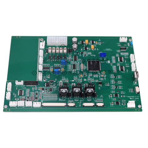
Achieving cost-effective PCBA workflows requires a strategic balance between PCB assembly efficiency and quality control. By integrating automated pick-and-place systems with intelligent material handling, manufacturers can reduce labor costs while maintaining precision in PCBA production. Real-time monitoring tools further optimize resource allocation, enabling dynamic adjustments to minimize waste during printed circuit board fabrication.
A critical factor lies in streamlining component procurement through vendor consolidation and bulk purchasing agreements. This approach not only lowers material costs but also reduces lead times, ensuring seamless integration with PCB assembly timelines. Additionally, adopting design-for-manufacturing (DFM) principles early in the process helps eliminate rework by identifying potential issues before they escalate into costly errors.
Advanced PCBA workflows now leverage predictive analytics to forecast maintenance needs for assembly equipment, preventing unplanned downtime. Pairing this with statistical process control (SPC) methods ensures consistent output quality without over-investing in redundant inspections. For high-volume orders, modular production lines allow rapid reconfiguration, scaling operations efficiently to meet fluctuating demand.
Finally, implementing closed-loop feedback systems between testing phases and assembly stages creates a self-correcting workflow. This iterative refinement reduces defect rates in printed circuit board outputs while aligning with lean manufacturing principles, ultimately driving down per-unit costs without compromising reliability.
Smart Integration in PCB Assembly
Modern PCB assembly workflows increasingly rely on smart integration of advanced technologies to bridge design, component placement, and testing phases. By embedding IoT-enabled sensors and AI-driven analytics into PCBA production lines, manufacturers gain real-time visibility into process variables like solder paste viscosity and thermal profiles. This connectivity enables automated adjustments, minimizing deviations before they escalate into defects. For instance, machine learning algorithms analyze historical assembly data to predict component misalignments, triggering corrective actions in pick-and-place systems.
A critical advantage lies in unifying automated optical inspection (AOI) systems with centralized control platforms. These integrated setups flag anomalies—such as insufficient solder joints or misplaced capacitors—during early stages, reducing rework cycles by up to 40%. Additionally, cloud-based collaboration tools allow cross-functional teams to synchronize design revisions with assembly parameters, ensuring seamless transitions from prototyping to mass production.
Such smart integration not only accelerates throughput but also fortifies traceability. Each PCBA unit carries digital identifiers, linking it to granular production data for compliance audits or failure analysis. By harmonizing hardware precision with software intelligence, manufacturers achieve scalable, error-resilient workflows that align with evolving industry demands—all while preserving cost-efficiency across high-mix, low-volume production runs.
Boosting PCB Manufacturing Quality
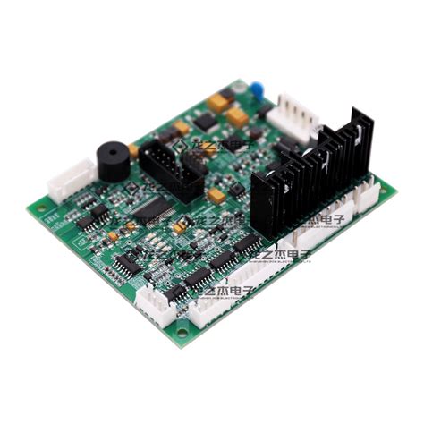
Enhancing quality in PCB assembly requires a multilayered approach that combines rigorous testing protocols with intelligent process optimization. At the core of PCBA quality improvement lies the integration of automated optical inspection (AOI) systems, which detect microscopic defects like solder bridging or misaligned components with sub-millimeter precision. Pairing AOI with X-ray inspection ensures even hidden flaws, such as voids in ball grid arrays (BGAs), are identified before final product validation.
To minimize variability, manufacturers are adopting statistical process control (SPC) tools that monitor critical parameters—solder paste deposition thickness, reflow oven temperature profiles, and component placement accuracy—in real time. These metrics feed into PCBA workflows, enabling predictive adjustments that preemptively address deviations. For instance, machine learning algorithms analyze historical defect data to refine placement algorithms, reducing rework rates by up to 30% in high-volume production.
Material selection also plays a pivotal role. High-reliability substrates, low-voiding solder pastes, and moisture-resistant conformal coatings collectively extend the lifespan of assembled boards. By aligning PCB assembly practices with ISO 9001 and IPC-A-610 standards, manufacturers ensure consistency across batches while meeting stringent industry benchmarks. This holistic focus on precision, traceability, and material excellence transforms quality from a checkpoint into a continuous improvement cycle.
Advanced PCBA Process Techniques
Modern PCB assembly workflows leverage high-precision automation to address the complexities of PCBA manufacturing. By integrating surface-mount technology (SMT) with robotic pick-and-place systems, manufacturers achieve micron-level accuracy in component placement, reducing manual intervention by up to 90%. Advanced 3D solder paste inspection (SPI) tools further enhance quality control, detecting insufficient or excess solder deposits before reflow processes. For multilayer boards, laser-drilled microvias enable compact designs while maintaining signal integrity, critical for high-frequency applications like IoT devices or automotive electronics.
Real-time analytics embedded in PCBA production lines monitor variables such as thermal profiles and humidity, dynamically adjusting parameters to prevent defects. Additionally, machine learning algorithms analyze historical assembly data to predict potential failure points, enabling preemptive corrections. These techniques align with automated optical inspection (AOI) systems, which perform 100% post-assembly verification, ensuring zero-defect output even in high-volume batches.
To sustain efficiency, manufacturers adopt modular fixturing for rapid changeovers between product variants, minimizing downtime. This approach, combined with closed-loop feedback from testing stages, creates a self-optimizing PCB assembly ecosystem. Such advancements not only streamline workflows but also lay the foundation for scalable, cost-effective production—a critical advantage in industries demanding both precision and agility.
Maintaining Automated PCB Standards
Consistent adherence to automated PCB assembly standards ensures long-term reliability and scalability in PCBA production. Modern facilities employ real-time monitoring systems to track parameters like solder paste deposition accuracy and component placement alignment, minimizing deviations during high-speed operations. Integrating machine learning algorithms with automated optical inspection (AOI) tools enables proactive identification of anomalies, such as solder bridging or misaligned ICs, before they escalate into costly rework.
To sustain these benchmarks, manufacturers implement automated calibration protocols for pick-and-place machines and reflow ovens, ensuring thermal profiles remain within ±2°C tolerances. This precision is critical for handling temperature-sensitive components in advanced PCBA designs, such as high-density interconnects (HDIs) or flex-rigid boards. Additionally, standardized data exchange formats—like IPC-2581—facilitate seamless communication between PCB assembly equipment and enterprise resource planning (ERP) systems, reducing manual intervention.
Regular audits of automated workflows using statistical process control (SPC) metrics further validate compliance with industry certifications like ISO 9001. By embedding predictive maintenance schedules into robotic systems, downtime is reduced by up to 30%, reinforcing operational continuity. These practices not only uphold quality but also align with evolving regulatory requirements, positioning PCBA manufacturers to adapt swiftly to emerging technologies while maintaining cost discipline.
Conclusion
The evolution of PCB assembly processes underscores the importance of harmonizing automation with rigorous quality control to achieve uncompromising precision in PCBA manufacturing. As demonstrated throughout this analysis, integrating advanced technologies—such as AI-driven inspection systems and real-time data analytics—enables manufacturers to minimize defects while accelerating production timelines. By implementing error reduction techniques like automated optical inspection (AOI) and in-circuit testing (ICT), businesses can maintain cost-effective workflows without sacrificing reliability.
Moreover, the strategic adoption of smart integration tools ensures seamless coordination between design, component placement, and testing phases, further enhancing manufacturing efficiency. These practices not only align with industry benchmarks but also future-proof operations against evolving technical demands. As the PCBA sector continues to innovate, prioritizing scalable solutions and continuous process optimization will remain pivotal for sustaining competitive advantage. Ultimately, the convergence of automation, precision, and adaptive workflows defines the pathway toward next-generation PCB assembly excellence.

Frequently Asked Questions
How does automation improve efficiency in PCB assembly?
Automation minimizes manual intervention in PCBA processes, accelerating component placement and soldering. Advanced machinery ensures consistent accuracy, reducing time spent on rework and calibration.
What role does precision testing play in manufacturing workflows?
Precision testing identifies defects early in PCB assembly, preventing costly downstream errors. Techniques like automated optical inspection (AOI) and in-circuit testing (ICT) validate electrical performance and solder integrity.
Can cost-effective production coexist with high-quality standards?
Yes. Optimized PCBA workflows integrate lean manufacturing principles, reducing material waste. Bulk purchasing of components and predictive maintenance further lower operational costs without compromising quality.
How are errors reduced in modern PCB manufacturing?
Error reduction relies on AI-driven design validation and real-time monitoring during PCB assembly. These systems flag inconsistencies, enabling immediate corrections before final production stages.
What makes smart integration critical for advanced PCBA?
Smart integration connects design software, assembly machines, and testing systems into a unified workflow. This seamless data exchange enhances traceability and reduces bottlenecks in complex PCBA projects.
How do manufacturers maintain quality control in automated setups?
Regular calibration of equipment, coupled with statistical process control (SPC), ensures adherence to PCB assembly standards. Automated reporting tools track performance metrics for continuous improvement.
Why should companies prioritize automation in PCBA?
Automation boosts throughput, ensures repeatability, and scales with demand. It also mitigates human error, making it indispensable for high-volume PCB manufacturing environments.
Explore Customized PCB Assembly Solutions
For tailored PCBA strategies that align with your production goals, please click here to consult our experts.


