Advanced Strategies for Streamlined PCB Design and Fabrication
Key Takeaways
Effective integration of PCB design and fabrication processes hinges on aligning engineering decisions with manufacturing realities. By adopting Design for Manufacturability (DFM) principles early, teams can preempt common pitfalls such as misaligned vias or insufficient clearances, which often lead to costly rework. For instance, optimizing trace widths and pad sizes during the design phase ensures compatibility with PCB assembly (PCBA) equipment, reducing errors in high-volume production.
Tip: Always validate designs against your manufacturer’s DFM checklist before finalizing layouts to avoid delays.
Smart material selection plays a dual role in cost reduction and performance enhancement. Choosing substrates with appropriate thermal stability or dielectric properties minimizes waste and ensures reliability in demanding environments. Additionally, leveraging automated PCB tools—like AI-driven routing software—accelerates design iterations while maintaining precision. Prototyping remains critical; rigorous prototype validation uncovers hidden flaws, such as signal integrity issues, before mass production.
For cost-effective fabrication, consider standardizing component packages and panelizing designs to maximize material utilization. Collaborative workflows between design and manufacturing teams further streamline timelines, ensuring seamless transitions from PCB design to PCBA. By prioritizing manufacturability and fostering cross-functional communication, organizations can achieve faster time-to-market without compromising quality.

Integrating PCB Design and Fabrication Processes
Effective PCB design requires seamless coordination between engineering teams and manufacturing partners from the earliest stages. By aligning design for manufacturability (DFM) principles with fabrication capabilities, engineers can preemptively address potential flaws in material compatibility or thermal management. For instance, integrating PCB assembly requirements—such as component spacing for automated pick-and-place systems—directly into layout software reduces rework during PCBA stages.
Modern workflows leverage collaborative digital platforms to synchronize design iterations with fabrication constraints, enabling real-time feedback on trace widths, layer stackups, and solder mask specifications. This proactive approach minimizes mismatches between theoretical designs and physical production limits, particularly when working with high-density interconnect (HDI) boards or mixed-signal layouts.
Additionally, adopting standardized component libraries approved by fabrication partners ensures consistency across PCB assembly processes. Designers should prioritize materials with verified supply chain availability to avoid delays, while simulation tools can validate manufacturability before prototyping. Such integration not only accelerates timelines but also establishes a foundation for scalable PCBA workflows, where design choices directly influence yield rates and post-production testing efficiency.
DFM Guidelines for Error-Free PCB Manufacturing
Implementing Design for Manufacturing (DFM) principles ensures seamless transitions from PCB design to fabrication while minimizing production risks. By aligning design choices with manufacturing capabilities, engineers can avoid common pitfalls such as misaligned vias or insufficient solder mask clearance. Key DFM considerations include optimizing trace widths for current load, maintaining adequate spacing between components, and adhering to fab-specific tolerance thresholds.
A critical aspect involves validating designs against PCB assembly (PCBA) requirements early in the process. For instance, component footprints must match pick-and-place machine specifications to prevent placement errors during PCBA. The table below outlines essential DFM parameters for error reduction:
| DFM Parameter | Recommended Value | Impact on Fabrication |
|---|---|---|
| Minimum Trace Width | ≥ 0.15mm | Prevents etching defects |
| Drill-to-Copper Clearance | ≥ 0.25mm | Avoids short circuits |
| Annular Ring Size | ≥ 0.05mm | Ensures via reliability |
| Solder Mask Expansion | ≥ 0.1mm | Enhances solder adhesion |
Additionally, designers should prioritize symmetrical component placement to balance thermal stresses during PCBA reflow soldering. Collaborating with fabrication partners to review material selection and layer stack-ups further reduces prototype rejection rates. By integrating DFM checks into CAD workflows, teams can achieve first-pass success in PCB fabrication, slashing costs linked to design iterations and accelerating time-to-market.
Smart Material Selection to Reduce Costs
Strategic material selection forms the backbone of cost-efficient PCB fabrication and pcb assembly. By aligning substrate choices with performance requirements and manufacturing capabilities, engineers can avoid over-specification while maintaining reliability. For instance, opting for standard FR-4 laminates instead of high-frequency alternatives for non-critical applications slashes material costs by up to 40% without compromising functionality.
Integrating DFM guidelines early in the design phase ensures compatibility with automated pcba workflows. Materials with consistent dielectric properties and thermal stability reduce rework during pcb assembly, while solder mask selections that match high-volume production processes minimize curing delays. Collaborating with fabrication partners to identify cost-effective alternatives—such as lead-free finishes or standardized copper weights—further optimizes budgets.
Bulk purchasing agreements for frequently used substrates and leveraging supplier expertise in thermal management solutions also contribute to savings. However, balancing cost with durability remains critical: subpar materials may lower upfront expenses but increase failure rates in field applications. By validating material performance through prototype testing and lifecycle analysis, teams achieve a sustainable balance between economy and quality in PCB fabrication.
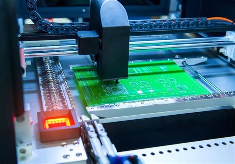
Accelerating Production with Automated PCB Tools
The adoption of automated PCB tools is revolutionizing how engineers bridge the gap between design and pcb assembly. Advanced software solutions, such as automated routing algorithms and component placement optimizers, enable rapid iteration of complex layouts while adhering to DFM guidelines. By integrating PCBA-specific workflows early in the design phase, teams can preemptively address manufacturability constraints, reducing post-production revisions.
Modern automated optical inspection (AOI) systems further streamline pcb fabrication by identifying defects like soldering errors or trace misalignments in real time. These tools minimize manual intervention, accelerating timelines by up to 40% in high-volume production. Additionally, simulation-driven platforms validate thermal and signal integrity performance before physical prototyping, ensuring compatibility with pcb assembly requirements.
Transitioning to automated systems also enhances collaboration between design and fabrication teams. Cloud-based PCBA project management tools synchronize design files, material specifications, and testing protocols, eliminating bottlenecks caused by version mismatches. As industries prioritize faster time-to-market, leveraging automated PCB tools becomes critical for maintaining competitiveness without compromising on cost-efficiency or quality. This approach naturally sets the stage for exploring prototype validation strategies in subsequent sections.

Minimizing Errors via Prototype Validation
Prototype validation serves as a critical checkpoint in the PCB design fabrication lifecycle, bridging the gap between theoretical designs and physical production. By rigorously testing early-stage prototypes, engineers can identify functional discrepancies, signal integrity issues, or PCB assembly flaws that may not be evident in simulation tools. For instance, validating a PCBA prototype through functional testing, thermal stress analysis, and design-for-manufacturability (DFM) audits ensures alignment between design intent and fabrication realities.
Transitioning from iterative design adjustments to full-scale production becomes smoother when validation phases incorporate real-world environmental factors, such as vibration or humidity. This step also highlights opportunities to refine material selection or optimize component placement to avoid rework during mass production. Automated inspection tools, like AOI (Automated Optical Inspection), further enhance accuracy by cross-referencing prototype measurements against original design specifications.
Collaboration between design and fabrication teams during validation is key. Sharing feedback on tolerances, solder mask alignment, or PCBA assembly challenges fosters a unified approach to error reduction. By addressing issues at this stage, manufacturers minimize costly delays and ensure seamless scalability, ultimately supporting the broader goal of accelerating time-to-market while maintaining quality standards.
Cost-Effective Strategies for PCB Fabrication
Achieving cost efficiency in PCB fabrication requires a holistic approach that balances technical precision with strategic resource management. A foundational step involves optimizing panelization layouts to maximize material utilization, reducing waste while maintaining proper spacing for PCBA processes. Implementing design-for-manufacturing (DFM) principles early in the development cycle helps identify potential fabrication bottlenecks, such as overly tight tolerances or non-standard via sizes, which can inflate costs during PCB assembly.
Leveraging standardized materials and finishes—such as FR-4 substrates or HASL coatings—can lower expenses without compromising reliability. For high-volume orders, collaborating with fabrication partners to negotiate bulk pricing for raw materials or shared tooling setups further enhances savings. Additionally, integrating automated optical inspection (AOI) systems during PCBA stages minimizes rework costs by detecting soldering defects or component misalignments in real time.
Transitioning to modular designs that reuse validated circuit blocks across multiple projects streamlines both fabrication and PCB assembly, cutting down on iterative testing phases. Finally, adopting hybrid manufacturing models—combining in-house prototyping with outsourced mass production—ensures flexibility while maintaining cost control. These strategies, when aligned with collaborative workflows, create a seamless bridge between design intent and fabrication execution.

Optimizing Layouts for Manufacturability
Effective PCB design requires balancing electrical performance with manufacturability to ensure seamless transition to PCB assembly. A well-optimized layout minimizes fabrication complexities by adhering to DFM (Design for Manufacturing) guidelines, such as maintaining proper trace widths, spacing, and pad sizes. For instance, aligning component orientations uniformly simplifies PCBA processes, reducing placement errors during automated soldering.
Integrating thermal management strategies—like avoiding clustered high-power components—prevents warping during reflow, while strategic via placement enhances signal integrity without compromising layer stackup feasibility. Designers should also prioritize standardized footprint libraries to eliminate mismatches between CAD models and physical components, a common source of PCB assembly delays.
Collaboration with fabrication partners early in the design phase helps identify constraints, such as minimum drill sizes or copper balancing requirements. By embedding DFM checks into the design workflow—using tools that flag issues like acid traps or insufficient annular rings—teams can preemptively address flaws before prototyping. This proactive approach not only accelerates PCBA timelines but also reduces costs linked to rework, ensuring designs are both functional and economically viable for mass production.
Streamlining Timelines with Collaborative Workflows
Effective collaboration between PCB assembly teams and design engineers is critical for accelerating project timelines. By implementing cloud-based design platforms, stakeholders can share real-time updates, reducing the lag between design iterations and PCBA (Printed Circuit Board Assembly) feedback. For instance, integrating design for manufacturing (DFM) checks directly into collaborative tools allows engineers to address potential fabrication issues before prototypes are built, eliminating costly rework cycles.
Cross-functional workflows also enable seamless material sourcing alignment. When procurement teams participate early in the design phase, they can flag supply chain bottlenecks or suggest alternative components that meet both performance and PCB assembly requirements. This proactive coordination minimizes delays caused by last-minute substitutions.
Automated version control systems further enhance efficiency by ensuring all stakeholders reference the latest design files. Such tools reduce miscommunication risks, particularly when handling complex PCBA layouts with multilayer configurations. Additionally, shared dashboards tracking progress metrics—such as design freeze dates or fabrication lead times—create accountability and transparency across teams.
By fostering a culture of continuous feedback, organizations can compress development cycles while maintaining quality standards, ensuring that collaborative workflows become a cornerstone of modern PCB design fabrication strategies.
Conclusion
The integration of PCB design and fabrication processes represents a strategic imperative for modern electronics manufacturing. By aligning DFM guidelines with intelligent material choices, teams can preemptively address potential bottlenecks in PCB assembly, ensuring smoother transitions from prototyping to full-scale production. Emphasizing collaboration between designers and PCBA specialists not only reduces iterative delays but also strengthens error detection through real-time feedback loops. Leveraging automated tools for layout optimization and validation further minimizes rework, while prototype testing serves as a critical checkpoint to validate manufacturability before committing to high-volume runs. Ultimately, a unified approach to PCB fabrication—one that prioritizes cost-efficiency, material suitability, and process scalability—enables organizations to deliver robust, market-ready products without compromising timelines. This synergy between design intent and production realities underscores the importance of treating PCB assembly not as a standalone phase but as an extension of the engineering lifecycle.
FAQs
How does integrating PCB assembly considerations during design improve outcomes?
Incorporating PCBA requirements early in the design phase ensures alignment with manufacturing capabilities, reducing post-design revisions. By adhering to DFM guidelines, designers avoid issues like improper component spacing or incompatible materials, which can delay PCB fabrication timelines.
What role does material selection play in cost-effective PCB fabrication?
Choosing materials like FR4 for standard applications or high-frequency substrates for specialized needs directly impacts both performance and budget. Intelligent selection minimizes waste and avoids over-engineering, aligning with cost-effective strategies outlined in the design phase.
Why is prototype validation critical for minimizing errors?
Prototyping identifies flaws in PCB assembly workflows before mass production. For example, testing thermal management or signal integrity early prevents costly rework. Combined with automated optical inspection (AOI) tools, this step ensures adherence to PCBA quality standards.
How do collaborative workflows accelerate production timelines?
Shared digital platforms allow real-time feedback between designers and PCB fabrication teams. This integration reduces miscommunication, enabling faster iterations and ensuring manufacturability is prioritized from the initial layout stage.
Ready to Optimize Your PCB Process?
For expert guidance on PCB assembly and seamless integration of design-to-fabrication workflows, please click here to explore tailored solutions.