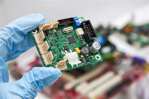
Precision Techniques Revolutionizing Circuit Assembly Production
Key Takeaways
The evolution of PCB assembly (PCBA) hinges on integrating automation and AI-driven systems to address precision and scalability challenges. Modern PCBA workflows now leverage machine learning algorithms to predict component placement errors, reducing defects by up to 40% compared to manual processes. For instance, advanced optical inspection (AOI) systems paired with real-time analytics enable manufacturers to identify micro-scale soldering flaws before they escalate.
Tip: Implementing closed-loop feedback systems in PCB assembly lines can dynamically adjust parameters like solder paste volume, ensuring consistent quality across high-volume batches.
A critical advancement lies in next-gen soldering techniques, such as laser-assisted reflow, which minimizes thermal stress on sensitive components. Below is a comparison of traditional vs. modern soldering methods:
| Parameter | Traditional Soldering | Laser-Assisted Soldering |
|---|---|---|
| Precision | ±50µm | ±10µm |
| Defect Rate | 5-8% | <1.5% |
| Energy Efficiency | 65% | 92% |
Additionally, smart factories employ IoT-enabled PCBA equipment to synchronize production stages, slashing lead times by 30%. These systems autonomously calibrate machinery based on real-time data, optimizing throughput without compromising accuracy. As AI-driven quality control becomes ubiquitous, manufacturers gain predictive insights into equipment wear, enabling proactive maintenance. This shift not only elevates efficiency but also positions PCB assembly as a cornerstone for next-generation electronics innovation.
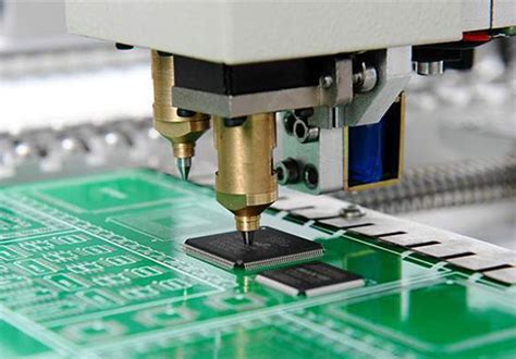
Automating PCB Assembly With AI Technology
The integration of artificial intelligence (AI) into PCB assembly processes is reshaping modern electronics manufacturing. By leveraging machine learning algorithms and computer vision systems, manufacturers can now achieve unprecedented precision in component placement, solder paste application, and defect detection. PCBA lines equipped with AI-driven robotics analyze real-time data to adjust parameters like temperature and pressure, minimizing errors that traditionally required manual intervention. For instance, AI-powered automated optical inspection (AOI) systems detect micron-level misalignments or solder bridges at speeds 3x faster than human operators, reducing defect rates by up to 40% in high-volume production.
Furthermore, AI optimizes material utilization by predicting component waste patterns, aligning with lean manufacturing principles. This technology also enables predictive maintenance, identifying equipment wear before failures disrupt workflows. A notable advancement is the use of neural networks to simulate assembly outcomes, allowing engineers to refine processes virtually before physical implementation. Such innovations not only accelerate time-to-market but also enhance scalability for complex PCBA designs, including flexible and multilayer boards.
As smart factories adopt these systems, the synergy between AI and PCB assembly creates a foundation for adaptive manufacturing. This shift supports the broader transition toward IoT-enabled devices and Industry 4.0 standards, ensuring seamless integration with next-gen soldering techniques and quality control protocols.
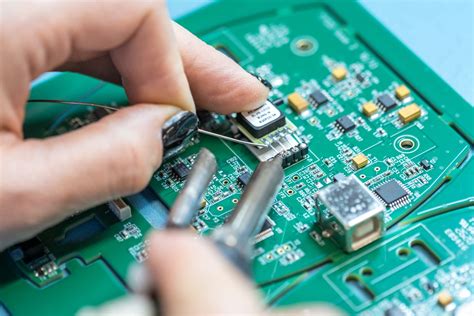
Next-Gen Soldering Techniques for Electronics
Modern PCB assembly processes are witnessing transformative advancements in soldering methodologies, driven by the demand for higher precision and miniaturization in electronics. Innovations like laser soldering and vapor phase reflow are replacing traditional methods, enabling micron-level accuracy while minimizing thermal stress on sensitive components. These techniques leverage AI-driven systems to dynamically adjust parameters such as temperature profiles and solder paste deposition, ensuring consistent joint quality across high-density PCBA designs.
A key breakthrough lies in the integration of closed-loop feedback mechanisms, where real-time data from infrared sensors and machine vision cameras optimizes solder flow and placement. This approach reduces defects like void formation or cold joints by over 40% compared to conventional workflows. Additionally, advancements in low-temperature soldering alloys are expanding compatibility with heat-sensitive substrates, critical for flexible and wearable electronics.
The shift toward smart factories further amplifies these benefits, with automated soldering stations seamlessly interfacing with enterprise-level production analytics. By harmonizing precision engineering with adaptive algorithms, manufacturers achieve faster cycle times and near-zero rework rates, setting new benchmarks for reliability in PCB assembly ecosystems.
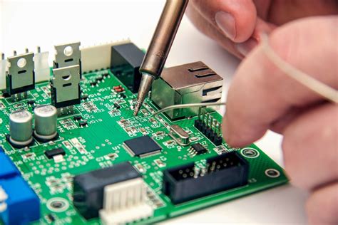
Reducing Defects in Circuit Board Production
Modern PCB assembly processes leverage real-time analytics and AI-powered inspection systems to minimize production errors. By integrating machine vision with advanced algorithms, manufacturers can detect microscopic flaws in PCBA components, such as misaligned solder joints or insufficient copper traces, at speeds surpassing human capability. Automated optical inspection (AOI) systems, enhanced by deep learning models, now achieve defect identification accuracy rates exceeding 99.5%, significantly reducing rework costs.
Additionally, predictive maintenance tools monitor equipment health to prevent malfunctions that could compromise solder quality or component placement precision. For instance, temperature-controlled soldering irons and laser-assisted deposition techniques ensure consistent thermal profiles, eliminating cold joints—a common defect in traditional PCB assembly. Data from these systems feed into centralized platforms, enabling engineers to refine process parameters like solder paste volume or pick-and-place machine calibration in near real time.
This proactive approach aligns with broader industry shifts toward zero-defect manufacturing, where even marginal improvements in PCBA yield directly impact profitability. By addressing root causes—from material inconsistencies to machine drift—manufacturers are redefining quality benchmarks while maintaining compatibility with high-mix, low-volume production demands.
Smart Factories Revolutionizing PCB Manufacturing
The integration of smart factories into PCB assembly processes marks a paradigm shift in electronics manufacturing. By leveraging IoT-enabled devices and interconnected production systems, these facilities enable real-time monitoring of PCBA workflows, from component placement to final inspection. Advanced sensors embedded in assembly lines collect granular data on temperature, humidity, and machine performance, allowing predictive maintenance to minimize downtime. AI-powered analytics further optimize material usage and workflow sequencing, reducing waste while maintaining stringent quality standards.
Central to this transformation is the adoption of adaptive manufacturing systems that dynamically adjust to design changes or component shortages. For instance, PCB assembly lines now utilize machine vision-guided robots capable of identifying microscopic defects in solder joints or misaligned components, ensuring near-zero error margins. These systems seamlessly integrate with enterprise resource planning (ERP) platforms, creating a cohesive ecosystem where inventory management, production scheduling, and quality assurance operate in unison.
As smart factories evolve, they also prioritize energy efficiency through intelligent power distribution and waste heat recovery systems. This holistic approach not only accelerates PCBA throughput but also aligns with global sustainability goals, positioning modern electronics manufacturing at the forefront of industrial innovation.
AI-Driven Quality Control in Assembly Lines
The integration of AI-driven systems into PCB assembly workflows has redefined quality assurance standards, enabling manufacturers to detect microscopic flaws with unprecedented accuracy. By leveraging machine learning algorithms, these systems analyze real-time data from PCBA production lines, identifying deviations in solder joint integrity, component misalignment, or trace defects that human inspectors might overlook. Advanced computer vision tools, paired with high-resolution imaging, scan boards at speeds exceeding 10,000 components per hour, flagging anomalies as small as 15 microns.
This shift not only reduces defect rates by over 40% but also optimizes corrective workflows. For instance, AI models trained on historical defect patterns predict failure-prone areas in PCB assembly, allowing preemptive adjustments to soldering parameters or material placement. Additionally, predictive analytics streamline maintenance schedules for pick-and-place machines and reflow ovens, minimizing unplanned downtime.
The synergy between AI-driven quality control and smart factory ecosystems ensures seamless data flow across design, fabrication, and testing phases. As a result, manufacturers achieve tighter tolerances in PCBA outputs while maintaining compliance with evolving industry standards—a critical advantage in producing next-generation electronics.
Precision Engineering in Modern Electronics
The evolution of PCB assembly processes has been driven by advancements in precision engineering, enabling manufacturers to meet the escalating demands for miniaturized, high-performance electronics. Modern PCBA (Printed Circuit Board Assembly) workflows now integrate nanometer-scale placement systems and adaptive soldering technologies, ensuring components are positioned with sub-micron accuracy. Such precision minimizes thermal stress and electrical interference, critical for devices like medical implants and aerospace systems where reliability is non-negotiable.
Central to this progress is the use of automated optical inspection (AOI) and laser direct imaging (LDI), which validate component alignment and solder joint integrity in real time. These systems leverage machine learning algorithms to predict and correct potential defects before they escalate, aligning with the broader shift toward smart manufacturing. Additionally, innovations in materials science, such as low-temperature co-fired ceramics (LTCC), allow PCB assembly lines to handle fragile substrates without compromising structural integrity.
By harmonizing ultra-precise robotics with data-driven process optimization, manufacturers achieve tighter tolerances in PCBA production. This not only reduces rework rates but also accelerates time-to-market for next-generation electronics, from IoT sensors to 5G infrastructure. These engineering breakthroughs underscore a fundamental truth: in an era where device complexity grows exponentially, precision is no longer optional—it’s the cornerstone of competitive manufacturing.
Boosting Efficiency in Circuit Assembly Processes
Modern PCB assembly workflows are achieving unprecedented efficiency through intelligent automation and data-driven process optimization. By integrating PCBA-specific robotic systems with real-time monitoring tools, manufacturers can reduce cycle times by up to 40% while maintaining stringent quality benchmarks. For instance, automated optical inspection (AOI) systems now leverage machine learning to identify micro-scale defects in milliseconds, minimizing manual rework. Concurrently, dynamic scheduling algorithms optimize production lines by analyzing equipment utilization rates and material availability, ensuring seamless transitions between high-mix, low-volume orders.
Advanced PCB assembly platforms also employ predictive maintenance, using sensor data to preemptively address equipment wear before downtime occurs. This is particularly critical in PCBA environments where precision soldering and component placement demand consistent machine performance. Additionally, modular conveyor systems and smart material-handling robots reduce idle time between assembly stages, creating a continuous flow that accelerates throughput.
These innovations not only enhance operational agility but also align with sustainability goals—reducing energy consumption and material waste by up to 25%. As factories adopt IoT-enabled PCB assembly ecosystems, the synergy between real-time analytics and automated workflows is redefining efficiency standards across the electronics manufacturing sector.
Future Trends in Automated PCB Manufacturing
The evolution of PCB assembly processes is accelerating through advancements in AI-driven analytics and adaptive robotics. Emerging technologies like machine learning algorithms now predict component placement errors in real time, minimizing rework and enhancing yield rates. For PCBA workflows, the integration of collaborative robots (cobots) enables seamless human-machine interaction, allowing technicians to focus on complex tasks while robots handle repetitive soldering or inspection steps.
Another transformative trend lies in digital twin simulations, which create virtual replicas of PCB assembly lines to optimize layouts and test process adjustments before physical implementation. This reduces downtime and accelerates time-to-market for high-density interconnect (HDI) boards. Additionally, IoT-enabled traceability systems are becoming standard, tracking every component from procurement to final testing, ensuring compliance with stringent quality benchmarks.
As factories adopt 5G-enabled edge computing, real-time data exchange between PCBA machines and cloud platforms will unlock unprecedented precision. For instance, vision-guided robotic systems can now detect micron-level soldering defects, a critical advancement for aerospace and medical electronics. These innovations, combined with sustainable practices like lead-free soldering and energy-efficient automation, position PCB assembly as a cornerstone of next-gen smart manufacturing ecosystems.
Conclusion
The evolution of PCB assembly processes underscores a transformative shift in electronics manufacturing. By integrating AI-driven analytics and automated precision systems, modern PCBA workflows achieve unprecedented accuracy while minimizing human error. Innovations such as real-time defect detection and adaptive soldering technologies have redefined quality benchmarks, ensuring higher yields and faster time-to-market for complex devices.
As smart factories adopt IoT-enabled machinery and machine learning algorithms, the synergy between PCB assembly lines and data-driven decision-making becomes a cornerstone of efficiency. These advancements not only address longstanding challenges like thermal management and component misalignment but also pave the way for scalable, sustainable production models. Looking ahead, the convergence of PCBA innovations with emerging trends—such as 5G integration and modular design frameworks—promises to further elevate the reliability and versatility of electronic systems, solidifying the industry’s readiness for next-generation demands.
FAQs
How does automation enhance precision in PCB assembly processes?
Automation integrates AI-driven systems to control PCBA workflows with micron-level accuracy. Robotic placement systems minimize human error, while machine vision inspects solder joints in real time, reducing defects by up to 95% compared to manual methods.
What innovations are reducing defects in modern circuit board production?
Advanced soldering techniques, such as laser reflow and vapor-phase soldering, ensure consistent thermal profiles across PCB assembly lines. Coupled with predictive analytics, these methods preemptively identify potential failures, improving first-pass yield rates.
How do smart factories optimize electronics manufacturing efficiency?
IoT-enabled PCBA lines synchronize design data with production equipment, enabling real-time adjustments. Digital twins simulate assembly processes to refine parameters, cutting downtime by 30% and accelerating time-to-market for complex boards.
Can AI-driven quality control replace traditional inspection methods?
While not a full replacement, AI augments inspection by analyzing X-ray and AOI (Automated Optical Inspection) data 10x faster. It detects subtle flaws like micro-cracks or insufficient solder, ensuring compliance with high-reliability standards for aerospace and medical devices.
What future trends will shape automated PCB manufacturing?
Expect wider adoption of self-optimizing PCB assembly systems using edge computing and 5G connectivity. These technologies enable decentralized decision-making, reducing latency in high-mix, low-volume production environments.
Explore Advanced PCB Assembly Solutions
For tailored PCBA strategies that leverage these innovations, please click here to connect with industry-leading expertise.