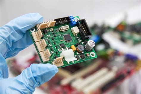
Optimizing PCB Assembly Board Manufacturing Techniques
Key Takeaways
Effective PCB assembly processes rely on balancing precision, automation, and material science to achieve optimal outcomes. Central to this is precision soldering, which ensures stable electrical connections while minimizing defects like cold joints or solder bridges. Pairing this with automated inspection systems—such as AOI (Automated Optical Inspection) or X-ray testing—enables real-time defect detection, reducing rework costs and accelerating production timelines.
Material selection plays a pivotal role in enhancing circuit reliability. High-performance substrates, low-voiding solder pastes, and thermally stable laminates mitigate risks of delamination or thermal stress. For PCBA (Printed Circuit Board Assembly) durability, factors like moisture resistance and coefficient of thermal expansion (CTE) must align with operational environments.
| Technique | Benefit | Application |
|---|---|---|
| AOI Systems | Defect detection accuracy >99.5% | Post-reflow inspection |
| Lead-Free Solders | Compliance with RoHS standards | High-temperature environments |
| FR-4 Substrates | Cost-effective thermal stability | Consumer electronics |
To boost manufacturing efficiency, integrating advanced automation—such as pick-and-place robots or AI-driven process optimization—reduces human error and cycle times. Streamlined workflows, combined with data-driven analytics, further refine yield rates and material utilization. By prioritizing these strategies, manufacturers can deliver PCB assembly boards that meet evolving industry demands for performance and scalability.
Precision Soldering for PCB Assembly
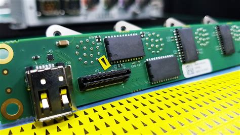
Precision soldering forms the backbone of high-quality PCB assembly, ensuring electrical connectivity and mechanical stability in PCBA (Printed Circuit Board Assembly). Modern techniques like reflow soldering and selective soldering enable micron-level accuracy, particularly for components with fine-pitch leads or miniature packages. Temperature control remains critical—excessive heat risks damaging sensitive ICs, while insufficient heat leads to cold joints.
Tip: Implement nitrogen-assisted soldering environments to reduce oxidation and improve wetting action, especially for lead-free solder alloys requiring higher melting points.
Advanced PCB assembly workflows now integrate laser-guided systems to align components before soldering, minimizing placement errors. For mixed-technology boards combining surface-mount (SMT) and through-hole components, dual-wave soldering systems ensure consistent coverage across diverse geometries. Post-soldering, automated optical inspection (AOI) validates joint integrity, flagging voids or bridging defects.
Material selection further influences outcomes: low-residue flux formulations prevent corrosion, while solder paste with Type 4 or 5 particle sizes enhances print resolution for ultra-fine traces. By optimizing these variables, manufacturers achieve PCBA outputs with <25 ppm defect rates, directly boosting end-product reliability in demanding applications like automotive or aerospace systems.
Automated PCB Inspection Systems
Modern PCB assembly processes increasingly rely on automated optical inspection (AOI) and X-ray inspection (AXI) systems to ensure manufacturing accuracy. These technologies replace time-consuming manual checks by scanning PCBA components for defects such as solder bridges, misaligned parts, or insufficient solder joints with micron-level precision. By integrating machine learning algorithms, inspection systems can adapt to complex board layouts, reducing false positives and identifying subtle flaws that might compromise circuit reliability.
A key advantage lies in real-time data collection, enabling manufacturers to trace defects back to specific stages in the PCB assembly line. For example, AOI systems paired with 3D solder paste inspection (SPI) tools can preemptively flag issues in stencil printing before components are placed. Similarly, AXI systems excel in verifying ball grid array (BGA) connections hidden beneath chips, a critical step for high-density PCBA designs.
These systems also support Industry 4.0 initiatives by feeding quality metrics into centralized analytics platforms. This闭环反馈 loop allows continuous refinement of assembly parameters, directly aligning with broader goals to enhance yield rates and minimize rework cycles. As PCB assembly scales toward miniaturization and higher complexity, automated inspection remains indispensable for balancing speed, cost, and reliability.
Material Selection for Reliable PCBs
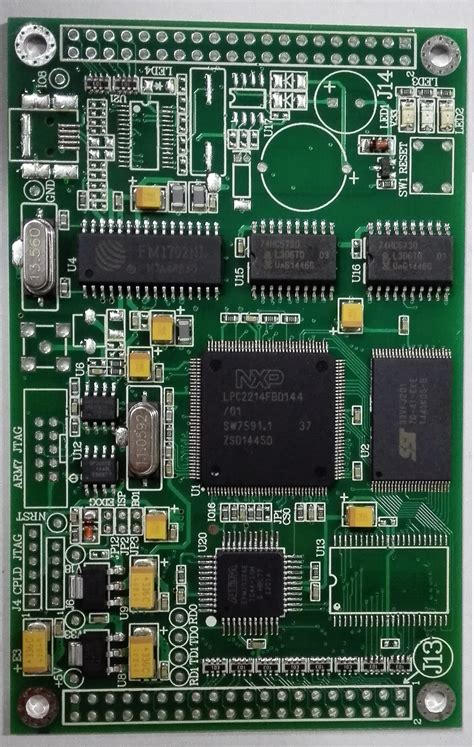
The foundation of durable PCB assembly lies in strategic material selection, which directly impacts performance, thermal management, and long-term reliability. High-frequency applications, for instance, demand substrates with low dielectric loss, such as Rogers or PTFE-based laminates, while standard PCBA projects often utilize cost-effective FR-4 materials. Copper weight and thickness must align with current-carrying requirements to prevent overheating or trace degradation. For harsh environments, halogen-free or polyimide substrates offer enhanced resistance to moisture, chemicals, and temperature fluctuations.
Solder mask quality also plays a critical role—epoxy-based or liquid photoimageable (LPI) options provide robust insulation and prevent electrochemical migration between closely spaced traces. Additionally, surface finishes like ENIG (Electroless Nickel Immersion Gold) or Immersion Silver ensure optimal solderability while minimizing oxidation risks during PCB assembly. Advanced manufacturers now integrate material databases with design-for-manufacturability (DFM) tools to automate compatibility checks, reducing errors in multilayer PCBA configurations. By prioritizing material synergy with operational demands, engineers can significantly enhance board longevity while streamlining production workflows.
Improving PCB Circuit Reliability
Ensuring long-term reliability in PCB assembly requires a multifaceted approach that addresses both design and manufacturing variables. A critical factor lies in optimizing thermal management strategies, as excessive heat remains a primary cause of circuit degradation. Implementing copper balancing techniques and selecting substrates with low coefficients of thermal expansion (CTE) can minimize warping during temperature fluctuations. Additionally, incorporating conformal coatings protects sensitive components from moisture, dust, and chemical exposure, particularly in harsh operating environments.
Advanced PCBA processes now leverage automated optical inspection (AOI) systems to detect micro-cracks or solder joint inconsistencies that manual inspections might miss. Pairing this with controlled impedance testing ensures signal integrity, especially in high-frequency applications. For mission-critical assemblies, accelerated life testing simulates years of operational stress within weeks, identifying potential failure points before mass production.
Material compatibility also plays a pivotal role. Using halogen-free laminates or high-Tg (glass transition temperature) materials enhances stability under thermal load, while gold-plated connectors reduce oxidation risks. By integrating these practices into PCB assembly workflows, manufacturers achieve a balance between durability and performance, directly impacting end-product longevity. This systematic approach not only mitigates field failures but also aligns with broader goals of reducing waste and improving sustainability in electronics manufacturing.
Boost PCB Manufacturing Efficiency
Enhancing efficiency in PCB assembly production requires a holistic approach that integrates process optimization with intelligent resource management. A critical starting point is adopting design for manufacturing (DFM) principles during the pcb assembly design phase, which minimizes rework by aligning layouts with production capabilities. For instance, optimizing component placement reduces solder bridging risks and accelerates PCBA workflows.
Automated systems, such as pick-and-place machines and automated optical inspection (AOI), further streamline workflows by reducing manual intervention. These tools ensure consistent placement accuracy while identifying defects early, preventing costly delays. Additionally, implementing data-driven analytics to monitor cycle times and yield rates enables manufacturers to pinpoint bottlenecks—like inefficient solder paste application or prolonged curing times—and apply corrective measures swiftly.
Material handling also plays a pivotal role. Standardizing component inventories and partnering with trusted suppliers reduces downtime caused by material shortages. For example, using lead-free solders with optimized melting profiles can shorten reflow cycles without compromising joint integrity. Similarly, selecting high-Tg laminates improves thermal stability, reducing warping during repeated thermal cycles.
Finally, integrating IoT-enabled monitoring into PCBA lines allows real-time tracking of equipment performance, enabling predictive maintenance. This not only extends machinery lifespan but also ensures uninterrupted production—a key factor in meeting tight deadlines. By harmonizing these strategies, manufacturers achieve a seamless balance between speed, cost, and quality, setting the stage for scalable growth in competitive markets.
Advanced PCB Assembly Automation
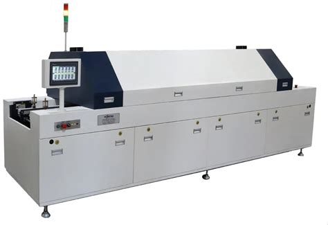
The integration of automated systems into PCB assembly workflows has revolutionized manufacturing precision and scalability. Modern pick-and-place robots, equipped with vision-guided alignment, achieve micron-level accuracy when positioning components on PCBA substrates, significantly reducing human error. These systems work in tandem with reflow soldering ovens that maintain exact thermal profiles, ensuring consistent joint quality across high-volume production runs.
A critical advancement lies in automated optical inspection (AOI) platforms, which leverage machine learning algorithms to detect microscopic defects—such as solder bridges or misaligned resistors—at speeds unattainable through manual checks. By pairing AOI with X-ray inspection for hidden connections in multilayer boards, manufacturers can preemptively address flaws before final testing.
Furthermore, smart material handling systems optimize component logistics, dynamically adjusting feeder configurations based on real-time demand. This agility minimizes downtime during product changeovers, aligning with lean manufacturing principles. As Industry 4.0 adoption grows, IoT-enabled PCB assembly lines now collect terabytes of process data, enabling predictive maintenance and continuous refinement of cycle times.
The shift toward PCBA automation not only accelerates throughput but also enhances repeatability for mission-critical applications, from aerospace to medical devices. By harmonizing robotic precision with adaptive software frameworks, manufacturers achieve tighter tolerances while maintaining flexibility to accommodate evolving design complexities.
Optimizing PCB Board Durability
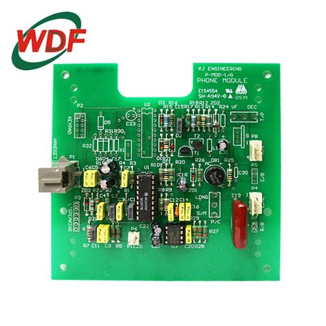
Enhancing the durability of PCB assembly boards requires a strategic focus on material resilience, environmental adaptability, and structural design. A critical starting point is selecting high-performance substrates such as FR-4 with high glass transition temperatures (Tg), which resist warping under thermal stress. For applications exposed to moisture or chemicals, protective conformal coatings—like acrylic or silicone-based layers—shield circuitry from corrosion and contaminants.
In PCBA processes, optimizing solder joint integrity is paramount. Using lead-free solder alloys with silver additives improves mechanical strength, reducing crack formation during thermal cycling. Additionally, implementing reinforced via structures—such as filled or capped vias—minimizes stress fractures in multilayer boards.
Environmental testing plays a pivotal role in validating durability. Accelerated life testing (ALT) simulates years of operational stress within weeks, identifying weak points in PCB assembly designs. Pairing this with vibration-resistant mounting techniques—like edge fasteners or adhesive underfills—ensures stability in high-motion environments.
Finally, balancing thermal management with mechanical robustness prevents premature failure. Integrating copper pours for heat dissipation while avoiding overly rigid layouts maintains flexibility. By aligning material choices, PCBA techniques, and stress-mitigation strategies, manufacturers achieve boards capable of enduring harsh conditions without compromising electrical performance.
Streamline PCB Production Processes
Efficient PCB assembly workflows depend on harmonizing design, fabrication, and testing phases to eliminate bottlenecks. A critical step involves adopting standardized design templates that align with PCBA (printed circuit board assembly) requirements, reducing rework caused by mismatched component footprints or layer configurations. Integrating automated material handling systems—such as pick-and-place machines with vision-guided precision—minimizes manual intervention while accelerating throughput.
Lean manufacturing principles further enhance efficiency. For example, implementing just-in-time (JIT) inventory management ensures components arrive precisely when needed, cutting storage costs and mitigating obsolescence risks. Additionally, real-time production monitoring tools—powered by IoT sensors or AI-driven analytics—identify inefficiencies like solder paste misapplication or conveyor delays, enabling immediate corrective actions.
Another essential strategy is process mapping, which visualizes workflow dependencies to pinpoint redundancies. By streamlining solder reflow profiles or optimizing stencil cleaning cycles, manufacturers can reduce cycle times by up to 20%. Collaboration between design and manufacturing teams also plays a pivotal role; leveraging DFM (design for manufacturability) guidelines ensures layouts are optimized for automated assembly, minimizing errors during PCBA stages.
Ultimately, a streamlined approach not only accelerates time-to-market but also elevates consistency across high-volume PCB assembly projects, ensuring scalability without compromising quality.
Conclusion
The evolution of PCB assembly manufacturing hinges on harmonizing precision, automation, and material innovation. By integrating high-accuracy soldering techniques with automated optical inspection (AOI) systems, manufacturers can minimize defects while maintaining consistency across PCBA batches. Strategic material selection—such as high-Tg laminates or halogen-free substrates—further enhances thermal resilience and long-term reliability, particularly in demanding environments.
Advancements in automated assembly lines have streamlined workflows, reducing human error and accelerating throughput. Pairing these systems with real-time analytics enables proactive adjustments, ensuring optimal performance during surface-mount technology (SMT) processes. Additionally, adopting predictive maintenance protocols for equipment like pick-and-place machines extends operational uptime, directly boosting PCB manufacturing efficiency.
As industries push for miniaturization and higher circuit densities, refining PCBA durability through advanced conformal coatings or underfill materials becomes critical. Collaborative efforts between design and production teams also ensure manufacturability is prioritized early, avoiding costly revisions. Ultimately, the convergence of these strategies not only elevates product quality but positions manufacturers to adapt swiftly to emerging technologies like AI-driven inspection or IoT-enabled supply chain management. The path forward demands continuous innovation, balancing cost-effectiveness with uncompromising standards in PCB assembly excellence.
FAQs
How does precision soldering impact pcb assembly quality?
Precision soldering ensures consistent electrical connections by minimizing defects like cold joints or bridging. Advanced techniques such as reflow soldering and selective soldering enhance accuracy, particularly for high-density PCBA designs.
What role do automated inspection systems play in pcb assembly?
Automated optical inspection (AOI) and X-ray systems detect microscopic flaws, such as misaligned components or insufficient solder. These systems reduce human error and improve yield rates in PCBA production, aligning with industry standards for reliability.
Why is material selection critical for pcb assembly board durability?
Materials like high-Tg laminates or halogen-free substrates resist thermal stress and environmental factors. Proper selection prevents delamination and ensures long-term performance, especially in applications requiring PCB circuit reliability.
How can manufacturers streamline pcba production processes?
Implementing lean manufacturing principles and integrating automated pick-and-place systems reduces cycle times. Real-time monitoring tools further optimize workflows, addressing bottlenecks in PCB manufacturing efficiency.
What steps enhance pcb assembly board longevity in harsh environments?
Conformal coatings and robust encapsulation methods protect against moisture, dust, and chemical exposure. Combined with rigorous thermal stress testing, these measures extend the operational lifespan of PCBA units.
Ready to Optimize Your PCB Assembly Process?
For tailored solutions in PCB assembly and PCBA manufacturing, please click here to explore advanced techniques and expert support.