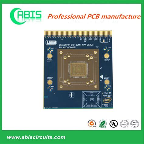
Expert Custom PCB Fabrication for Seamless Prototyping
Key Takeaways
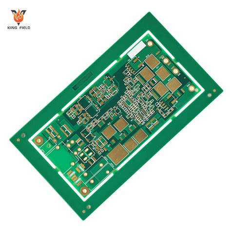
When navigating PCB manufacturing for prototyping, understanding core efficiency drivers helps optimize your development cycle. Leading PCB manufacturing companies now integrate 24-hour rapid prototyping with multi-process techniques—from laser drilling to automated optical inspection—to accelerate iterations while maintaining precision.
"Always request detailed breakdowns of PCB manufacturing cost structures early in discussions. This reveals hidden fees and helps align technical specs with budget constraints."
A key advantage lies in leveraging global networks that combine localized expertise with centralized quality control. This approach ensures consistent results whether you’re testing high-frequency RF designs or multi-layer boards. For startups, partnering with a PCB manufacturing business that offers end-to-end solutions—from design validation to final assembly—reduces logistical friction and accelerates time-to-market.
Cost efficiency extends beyond fabrication: consider panelization strategies and material alternatives like FR-4 substitutes to trim expenses without compromising performance. Transitioning from prototype to volume production? Prioritize vendors with scalable infrastructure and transparent communication protocols to avoid bottlenecks.
Tip: Use DFM (Design for Manufacturing) checks early to minimize redesigns. Most advanced providers include this service at no extra cost, ensuring your designs align with their PCB manufacturing capabilities.
Custom PCB Fabrication Speed Optimization
Accelerating PCB manufacturing timelines requires balancing technical precision with workflow efficiency. By leveraging advanced automation and intelligent design-for-manufacturing (DFM) checks, you can reduce turnaround times without compromising quality. Leading PCB manufacturing companies employ parallel processing for tasks like layer stacking and copper etching, cutting production cycles by up to 40% compared to traditional sequential methods.
When evaluating options, prioritize partners offering real-time design feedback—this prevents costly revisions and keeps projects on track. For instance, automated impedance matching tools minimize signal integrity issues early, avoiding delays during prototyping. Material selection also plays a critical role: using pre-certified substrates from trusted suppliers eliminates weeks-long qualification processes.
Managing PCB manufacturing cost while accelerating output hinges on scalable processes. Modular fabrication lines allow manufacturers to handle small-batch prototypes and high-volume runs simultaneously, ideal for iterative R&D. Additionally, geographically distributed facilities in PCB manufacturing business networks enable smarter logistics routing, ensuring faster delivery even for complex multilayer boards.
To further optimize timelines, explore speed optimization strategies that integrate design, testing, and assembly workflows. This end-to-end approach reduces handoff delays, ensuring your prototypes move seamlessly from CAD files to functional boards. By aligning your requirements with these methodologies, you maintain competitive agility while meeting tight development deadlines.
24-Hour Rapid Prototyping Service Benefits
When developing electronic systems, time-sensitive projects demand PCB manufacturing solutions that align with aggressive timelines. By leveraging 24-hour rapid prototyping, you gain critical advantages in compressing design validation cycles, allowing iterative testing without sacrificing momentum. Leading PCB manufacturing companies integrate automated workflows and advanced machinery to deliver functional prototypes within a single business day, ensuring design flaws are identified early—before committing to full-scale production.
This accelerated approach directly addresses unpredictable PCB manufacturing cost variables by minimizing material waste and reducing rework expenses. For startups or enterprises scaling their PCB manufacturing business, rapid prototyping enables faster market entry while maintaining rigorous quality benchmarks. Precision-controlled processes like laser drilling and automated optical inspection (AOI) ensure prototypes mirror final product specifications, eliminating discrepancies during mass production.
Moreover, the ability to test multiple design iterations within days—instead of weeks—strengthens R&D agility. Whether refining high-frequency signal integrity or optimizing thermal management, rapid prototyping transforms theoretical designs into tangible solutions. By aligning with partners offering round-the-clock services, you maintain project continuity across time zones, ensuring deadlines are met without compromising on technical requirements.
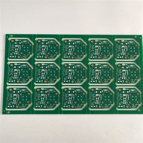
Multi-Process PCB Manufacturing Techniques
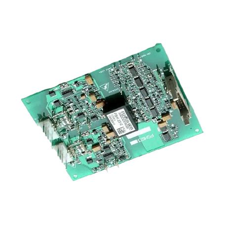
When developing custom prototypes, choosing PCB manufacturing companies that leverage multi-process capabilities ensures your designs meet exact specifications. Advanced techniques like laser direct imaging (LDI), automated optical inspection (AOI), and sequential lamination allow manufacturers to address complex layer stacks, tight tolerances, and high-density interconnects. These processes directly influence PCB manufacturing cost by minimizing material waste and reducing rework through precision-driven workflows.
For instance, combining electroless nickel immersion gold (ENIG) surface finishes with controlled-depth drilling enables robust performance in harsh environments, while impedance-controlled routing maintains signal integrity for high-frequency applications. By integrating these methods, PCB manufacturing becomes scalable—whether you’re iterating prototypes or transitioning to volume production.
Partnering with a PCB manufacturing business that offers end-to-end process integration also streamlines design adjustments. Real-time feedback loops between fabrication and engineering teams help optimize layouts for manufacturability, avoiding delays. This holistic approach ensures your project stays on budget and timeline, even when scaling across global supply chains.
Ultimately, multi-process techniques are not just about technical prowess—they’re about aligning fabrication strategies with your R&D goals to deliver seamless, reliable outcomes.
Global PCB Fabrication Support Networks
When developing complex electronics, accessing PCB manufacturing expertise across multiple regions ensures your project stays on track regardless of geographic constraints. Leading PCB manufacturing companies now operate interconnected facilities worldwide, combining localized production with centralized quality control. This approach minimizes delays caused by logistics bottlenecks while maintaining consistency in PCB manufacturing cost structures. By leveraging regional partnerships, you gain flexibility in material sourcing, compliance with local regulations, and faster turnaround for urgent prototyping needs.
Strategic alignment with global networks also mitigates risks inherent in relying on a single supplier. For instance, if one facility faces unexpected disruptions, your order can seamlessly shift to another location without compromising timelines. This resilience is critical for scaling a PCB manufacturing business, especially when balancing high-volume orders with niche custom requirements. Additionally, integrated communication platforms enable real-time collaboration between your team and international engineers, ensuring design specifications are met precisely.
Transitioning to a globally supported model doesn’t just expand your options—it future-proofs your supply chain, allowing you to adapt to shifting market demands while maintaining cost efficiency.
Precision Engineering for Seamless Prototypes
Achieving flawless prototypes begins with PCB manufacturing processes that prioritize micron-level accuracy. Modern PCB manufacturing companies leverage advanced laser direct imaging (LDI) systems and automated optical inspection (AOI) to ensure trace widths, spacing, and via placements align precisely with your design specifications. This technical rigor minimizes signal interference and thermal stress points, critical for high-frequency or high-power applications.
When evaluating PCB manufacturing cost, consider how precision engineering reduces iterative revisions. Tight tolerances (±0.05mm) in layer alignment and solder mask application prevent functional discrepancies, accelerating your path from prototype validation to mass production. Leading providers integrate design-for-manufacturability (DFM) feedback early, optimizing layouts to avoid costly redesigns.
For businesses scaling their PCB manufacturing business, partnering with certified suppliers ensures compliance with IPC-A-600 and ISO-9001 standards. These protocols govern material selection, surface finishes, and testing methodologies, guaranteeing reliability across industrial, automotive, or aerospace environments. By aligning engineering expertise with your project’s technical demands, you maintain control over both quality and timelines without compromising performance.
Streamline R&D With Expert PCB Solutions
When developing cutting-edge electronics, your R&D cycle hinges on partnering with PCB manufacturing companies that align with your technical and logistical requirements. Advanced design-for-manufacturability (DFM) feedback, coupled with scalable production workflows, ensures your prototypes transition seamlessly to full-scale production. By leveraging PCB manufacturing expertise, you mitigate risks like signal integrity issues or thermal mismanagement early in the design phase—saving weeks of iterative revisions.
| In-House Challenges | Expert Solutions |
|---|---|
| Limited material options | 50+ substrate choices for optimization |
| Manual DFM checks | AI-driven error detection algorithms |
| High PCB manufacturing cost | Volume-based pricing models |
Reputable providers integrate PCB manufacturing business insights directly into your development pipeline, offering real-time cost analytics and compliance tracking. This eliminates guesswork around IPC standards or RoHS certifications, allowing your team to focus on innovation rather than administrative overhead. For startups, this translates to faster time-to-market; for enterprises, it ensures consistent quality across global supply chains.
By adopting end-to-end collaboration tools, you gain visibility into every stage—from Gerber file validation to final inspection reports. Such transparency reduces unforeseen delays and aligns deliverables with your project milestones. Whether optimizing PCB manufacturing cost or navigating complex multilayer designs, expert partnerships turn prototyping bottlenecks into competitive advantages.
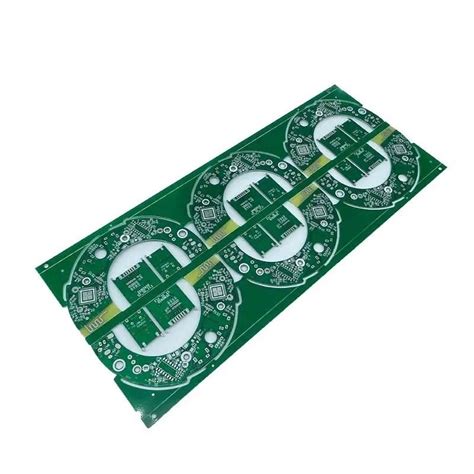
Cost-Effective Custom PCB Assembly Options
When balancing quality and affordability in PCB manufacturing, partnering with the right PCB manufacturing companies ensures you avoid unnecessary overheads without compromising performance. To reduce PCB manufacturing cost, consider optimizing design choices—such as panelization to maximize material usage—or selecting standard finishes over premium options where feasible. Many providers offer tiered pricing models that scale with order volume, allowing smaller businesses to compete in the PCB manufacturing business while maintaining budget flexibility.
Another strategy involves leveraging automated assembly processes, which minimize labor expenses and human error. Reputable suppliers often combine advanced machinery with bulk purchasing power to lower component costs, passing savings to you. However, cost-cutting shouldn’t sacrifice reliability—verify certifications like ISO or UL to ensure compliance with industry standards.
For prototypes or low-volume runs, shared panel services or "pooling" orders with other clients can further reduce per-unit expenses. Always request detailed breakdowns of PCB manufacturing cost structures to identify hidden fees, such as tooling or setup charges. By aligning your requirements with a manufacturer’s core capabilities—whether high-mix, low-volume or mass production—you streamline workflows and achieve predictable budgeting. This approach ensures your project stays on track financially while meeting technical specifications.
End-to-End PCB Design-to-Delivery Systems
When developing complex electronics, PCB manufacturing workflows demand seamless coordination from concept to final product. Modern PCB manufacturing companies leverage integrated design-to-delivery systems to eliminate bottlenecks, ensuring your prototypes transition smoothly from digital schematics to functional boards. By combining automated design verification with real-time supply chain tracking, these systems optimize timelines while maintaining rigorous quality checks.
Cost predictability becomes critical in this process. Advanced PCB manufacturing cost estimation tools analyze material choices, layer counts, and production volumes upfront, allowing you to balance performance requirements with budget constraints. For growing PCB manufacturing business operations, such end-to-end solutions enable rapid scaling—whether you’re iterating prototypes or preparing for mass production.
Moreover, these systems standardize communication across global partners, reducing errors caused by fragmented workflows. Whether you require rigid-flex boards or high-frequency substrates, unified platforms ensure design intent is preserved at every stage. This approach not only accelerates time-to-market but also minimizes rework, creating a foundation for consistent, repeatable results across projects.
Conclusion
When navigating the complexities of PCB manufacturing, your choice of partner determines not just project success but long-term scalability. Leading PCB manufacturing companies combine advanced technical expertise with transparent processes, ensuring your prototypes transition seamlessly into production. By prioritizing agile workflows and precision engineering, these providers mitigate risks associated with PCB manufacturing cost while maintaining compliance with global quality standards.
For businesses scaling their PCB manufacturing business, leveraging end-to-end solutions—from design validation to logistics—reduces bottlenecks in R&D cycles. Whether you require high-mix, low-volume prototypes or complex multi-layer boards, aligning with a partner that offers real-time collaboration and multi-process capabilities ensures your innovations reach the market faster. Remember: the right balance between technical proficiency and cost-efficiency unlocks competitive advantages in today’s fast-paced electronics landscape.
FAQs
How does PCB manufacturing affect prototype development timelines?
Advanced PCB manufacturing companies leverage automated processes and multi-process techniques to reduce lead times. When you partner with specialists offering 24-hour prototyping, design iterations become seamless, accelerating your R&D cycle.
What factors influence PCB manufacturing cost for custom projects?
Costs depend on material choices, layer counts, and production volumes. Reputable providers optimize PCB manufacturing business workflows to minimize waste, offering scalable pricing models that align with your project’s complexity and scale.
Can global teams collaborate effectively with PCB manufacturing partners?
Yes. Leading firms provide cloud-based design review tools and real-time progress tracking, ensuring alignment across time zones. Their global support networks simplify logistics, from material sourcing to final delivery.
How do you ensure precision in high-density PCB manufacturing?
Certified suppliers use laser-direct imaging and automated optical inspection to maintain tolerances below 0.1mm. This precision engineering guarantees functional prototypes that match your design specifications flawlessly.
Ready to Optimize Your PCB Workflow?
Streamline your next project with end-to-end solutions—from concept to production. Click here to explore tailored PCB manufacturing services and request a free quote today.