Ceramic PCB: A Comprehensive Guide
Introduction to Ceramic PCB
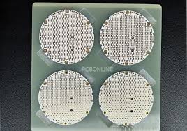
Printed Circuit Boards (PCBs) are essential components in modern electronics, providing mechanical support and electrical connections for electronic components. While traditional PCBs are made from materials like FR4, ceramic PCBs have gained significant attention due to their superior thermal, mechanical, and electrical properties.
Ceramic PCBs are constructed using ceramic materials such as alumina (Al₂O₃), aluminum nitride (AlN), and beryllium oxide (BeO). These materials offer excellent thermal conductivity, high-temperature resistance, and low thermal expansion, making them ideal for high-power and high-frequency applications.
This article explores the properties, manufacturing processes, advantages, disadvantages, and applications of ceramic PCBs.
Types of Ceramic PCB Materials
1. Alumina (Al₂O₃)
Alumina is the most commonly used ceramic material in PCBs due to its cost-effectiveness and good thermal conductivity (24-28 W/mK). It provides excellent electrical insulation and mechanical strength, making it suitable for LED lighting, power electronics, and automotive applications.
2. Aluminum Nitride (AlN)
Aluminum nitride offers superior thermal conductivity (140-180 W/mK), making it ideal for high-power applications such as RF modules, semiconductor packaging, and aerospace electronics. However, it is more expensive than alumina.
3. Beryllium Oxide (BeO)
Beryllium oxide has the highest thermal conductivity (250-300 W/mK) among ceramic PCB materials. However, due to its toxicity, its use is limited to specialized applications like military and aerospace electronics.
4. Silicon Carbide (SiC)
Silicon carbide is used in extreme environments due to its high thermal conductivity, chemical resistance, and mechanical durability. It is often employed in high-temperature and high-power applications.
Manufacturing Process of Ceramic PCBs
The production of ceramic PCBs involves several key steps:
1. Substrate Preparation
The ceramic material is shaped into thin sheets using techniques like tape casting or dry pressing. These sheets are then sintered at high temperatures to achieve the desired mechanical strength.
2. Metallization
Since ceramic is non-conductive, conductive traces are added through metallization techniques:
- Thick Film Technology: Conductive pastes (gold, silver, or copper) are screen-printed onto the ceramic substrate and fired at high temperatures.
- Direct Bonded Copper (DBC): A copper foil is bonded to the ceramic substrate under high temperature and pressure.
- Thin Film Technology: A thin layer of metal (e.g., sputtered or evaporated copper) is deposited and patterned using photolithography.
3. Laser Drilling and Via Formation
Microvias and holes are drilled using laser technology to create interconnections between layers in multilayer ceramic PCBs.
4. Component Assembly
Surface-mount devices (SMDs) and other components are soldered onto the ceramic PCB using high-temperature solders or conductive adhesives.
5. Testing and Quality Control
The final PCB undergoes electrical testing, thermal cycling, and inspection to ensure reliability and performance.
Advantages of Ceramic PCBs
1. High Thermal Conductivity
Ceramic materials dissipate heat more efficiently than traditional FR4, reducing the risk of overheating in high-power applications.
2. Excellent Electrical Insulation
Ceramic PCBs provide superior dielectric properties, minimizing signal loss in high-frequency circuits.
3. High-Temperature Resistance
They can withstand extreme temperatures (up to 1000°C for some materials), making them suitable for aerospace and automotive applications.
4. Low Thermal Expansion
Ceramic materials have a coefficient of thermal expansion (CTE) close to that of silicon, reducing stress in semiconductor packaging.
5. Miniaturization Capability
Ceramic PCBs support high-density interconnects, enabling compact and lightweight electronic designs.
6. Chemical and Corrosion Resistance
They are resistant to moisture, acids, and other harsh chemicals, ensuring long-term reliability.
Disadvantages of Ceramic PCBs
1. High Cost
Ceramic PCBs are more expensive than traditional FR4 PCBs due to material and manufacturing complexities.
2. Brittleness
Ceramic substrates are more fragile than organic PCBs, requiring careful handling during assembly.
3. Limited Availability
Specialized manufacturing processes mean fewer suppliers compared to conventional PCBs.
4. Complex Repairability
Repairing ceramic PCBs is difficult due to their rigid structure and high-temperature requirements.

Applications of Ceramic PCBs
1. LED Lighting
Ceramic PCBs are widely used in high-power LED modules due to their excellent heat dissipation.
2. Power Electronics
They are used in power converters, inverters, and motor drives where high thermal management is critical.
3. RF and Microwave Circuits
The low dielectric loss of ceramic materials makes them ideal for high-frequency applications like 5G communication and radar systems.
4. Automotive Electronics
Ceramic PCBs are used in electric vehicles (EVs), battery management systems (BMS), and engine control units (ECUs).
5. Aerospace and Defense
Their ability to withstand extreme conditions makes them suitable for satellites, avionics, and military electronics.
6. Medical Devices
Ceramic PCBs are used in implantable devices, diagnostic equipment, and high-precision sensors.
7. Semiconductor Packaging
They serve as substrates for IC packaging, providing thermal stability and electrical isolation.
Comparison: Ceramic PCB vs. FR4 PCB
| Property | Ceramic PCB | FR4 PCB |
|---|---|---|
| Thermal Conductivity | High (24-300 W/mK) | Low (~0.3 W/mK) |
| Temperature Resistance | Up to 1000°C | Up to 130°C |
| Dielectric Constant | Low (better for RF) | Higher (signal loss) |
| Mechanical Strength | Brittle | Flexible |
| Cost | High | Low |
| Applications | High-power, high-frequency | Consumer electronics |
Future Trends in Ceramic PCBs
1. Advanced Materials
Research is ongoing to develop new ceramic composites with improved thermal and electrical properties.
2. 3D Printed Ceramic PCBs
Additive manufacturing techniques are being explored to create complex ceramic PCB structures.
3. Integration with Flexible Electronics
Hybrid designs combining ceramic and flexible substrates could enable new applications in wearable technology.
4. Increased Adoption in 5G and IoT
The demand for high-frequency, high-reliability PCBs will drive growth in ceramic PCB usage.
Conclusion
Ceramic PCBs offer unparalleled performance in high-power, high-frequency, and high-temperature applications. Despite their higher cost and brittleness, their advantages in thermal management, electrical insulation, and reliability make them indispensable in industries like aerospace, automotive, and telecommunications.
As technology advances, ceramic PCBs will play an increasingly vital role in next-generation electronics, supporting innovations in 5G, IoT, and power-efficient systems. Engineers and designers must carefully evaluate their requirements to determine whether ceramic PCBs are the optimal solution for their applications.