The Importance and Best Practices of PCB Silkscreen
Introduction to PCB Silkscreen
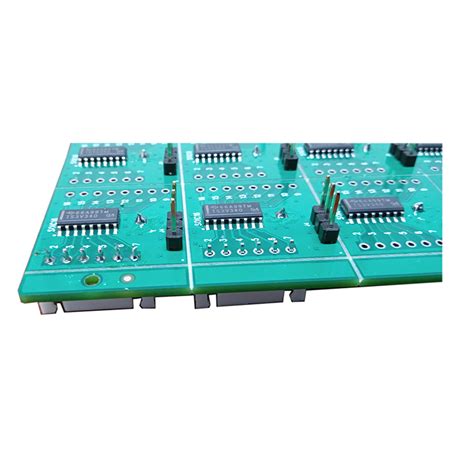
Printed Circuit Board (PCB) silkscreen, often referred to as “legend printing,” is a critical layer in PCB manufacturing that provides textual and symbolic information on the board’s surface. This non-conductive ink layer serves multiple purposes—from component identification to polarity markings and company logos. While often considered secondary to the copper layers that form the actual electrical connections, silkscreen plays an indispensable role in PCB assembly, testing, debugging, and maintenance.
Silkscreen technology has evolved significantly since the early days of PCB manufacturing. What began as simple hand-painted markings has transformed into sophisticated printing processes capable of producing high-resolution text and graphics on various board surfaces. In modern electronics manufacturing, where components are shrinking and board densities are increasing, the precision and clarity of silkscreen markings have become more important than ever.
Silkscreen Printing Methods
1. Manual Silkscreen Printing
The traditional method of silkscreen application involves using a stencil (or screen) made of fine mesh with the negative image of the desired markings. Ink is forced through the open areas of the stencil onto the PCB surface. While this method can produce satisfactory results for larger text and simple designs, it has several limitations:
- Resolution is limited to about 0.007 inches (0.18 mm)
- Registration accuracy may vary
- Not cost-effective for small batch production
- Difficult to maintain consistency across multiple boards
Despite these limitations, manual silkscreen printing remains in use for prototype boards or very large components where high precision isn’t critical.
2. Liquid Photo Imaging (LPI)
LPI represents a significant advancement in silkscreen technology, offering much higher resolution than traditional screen printing. This process involves:
- Applying a photosensitive epoxy ink across the entire board surface
- Exposing the ink to UV light through a photomask containing the silkscreen pattern
- Developing the board to remove unexposed areas
LPI offers several advantages:
- Resolution down to 0.004 inches (0.10 mm)
- Better adhesion to the board surface
- More consistent results
- Ability to print finer lines and smaller text
The trade-off is higher cost and more complex processing compared to manual screening, making LPI more suitable for medium to high volume production.
3. Direct Legend Printing (DLP)
The most advanced silkscreen method uses inkjet technology to print directly onto the PCB surface. This digital approach eliminates the need for physical stencils or masks, offering several benefits:
- Highest resolution (down to 0.002 inches or 0.05 mm)
- Excellent registration accuracy
- Quick changeover between designs
- Cost-effective for prototypes and small batches
- Ability to print variable information (like serial numbers)
DLP systems use specialized ink formulations that cure quickly and adhere well to various PCB surface finishes. While the equipment cost is higher than traditional methods, the flexibility and quality often justify the investment for manufacturers producing high-mix, low-volume boards.
Design Considerations for Effective Silkscreen
1. Text Size and Legibility
Choosing the appropriate text size is crucial for silkscreen effectiveness. General guidelines include:
- Minimum recommended character height: 0.040 inches (1.0 mm) for manual screening, 0.030 inches (0.75 mm) for LPI, and 0.020 inches (0.5 mm) for DLP
- Line width should be at least 15-20% of character height
- Maintain adequate spacing between characters (kerning) and between lines (leading)
Designers must balance readability with available board space, especially in dense layouts. Text that’s too small may become illegible after manufacturing or during assembly.
2. Placement and Orientation
Proper silkscreen placement prevents confusion during assembly and troubleshooting:
- Place reference designators adjacent to components, preferably in a consistent location (e.g., always to the right of resistors)
- Orient text to be read from one or two primary directions (avoid upside-down text)
- Keep markings clear of pads, vias, and component outlines
- Ensure polarity markings (for diodes, electrolytic capacitors, etc.) are unambiguous
- Place board identification information (part number, revision) in a consistent location
3. Color Selection
While white is the most common silkscreen color (offering good contrast against green solder mask), other colors are available:
- Black: Used on white or light-colored solder masks
- Yellow: Occasionally used on blue or red solder masks
- Clear: For a minimalist appearance (though less functional)
Contrast between silkscreen and solder mask is critical for readability. Some manufacturers offer custom colors at additional cost.
4. Content Guidelines
Effective silkscreen should include:
- Reference designators (R1, C5, U3, etc.)
- Polarity indicators (+/- for capacitors, cathode markers for diodes)
- Pin 1 indicators for ICs and connectors
- Test point identifications
- Warning symbols for high-voltage areas
- Board identification (part number, revision, date code)
- Company name/logo
- Regulatory markings (CE, UL, etc.) when required
Avoid including:
- Information that changes frequently (unless using DLP)
- Text under components (except when necessary for small parts)
- Excessive decorative elements that don’t serve functional purposes
Common Silkscreen Problems and Solutions
1. Poor Registration
Misalignment between silkscreen and board features can cause:
- Text overlapping pads or vias
- Markings appearing off-center
- Component identification becoming unclear
Solutions:
- Specify tighter registration tolerances with your manufacturer
- Allow adequate clearance around pads (typically 0.005-0.010 inches)
- Use fiducial markers to improve alignment accuracy
- Consider DLP for critical applications
2. Ink Adhesion Issues
Silkscreen that peels or flakes can lead to:
- Loss of important information
- Contamination during assembly
- Professional appearance degradation
Solutions:
- Specify appropriate ink type for your board surface finish
- Ensure proper surface preparation (cleaning)
- Consider LPI or epoxy-based inks for better adhesion
- Avoid placing silkscreen over irregular surfaces
3. Low Contrast/Legibility
Poor visibility makes assembly and troubleshooting difficult:
- Text blends into solder mask
- Fine details become indistinct
- Markings wear off easily
Solutions:
- Choose high-contrast color combinations
- Increase text size where possible
- Use bold fonts for better visibility
- Avoid placing silkscreen over textured surfaces
4. Incomplete or Missing Information
Critical omissions can cause assembly errors:
- Missing polarity markings
- Absent reference designators
- No board identification
Solutions:
- Implement thorough design reviews
- Use automated checks in PCB design software
- Create checklists for required silkscreen elements
- Verify with assembly team what information they need
Advanced Silkscreen Applications
1. High-Density Interconnect (HDI) Boards
As component sizes shrink and board densities increase, silkscreen faces new challenges:
- Ultra-fine pitch components (0402, 0201, or smaller) require microscopic markings
- Limited space for reference designators
- Need for alternative identification methods when direct marking isn’t possible
Solutions include:
- Using abbreviated reference designators
- Implementing numbered grids with separate legend
- Employing microscopic laser marking
- Utilizing multi-layer silkscreen approaches
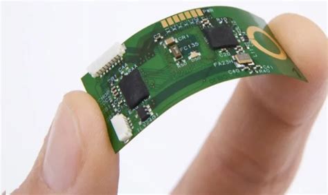
2. Flexible and Rigid-Flex PCBs
Special considerations apply for flexible circuits:
- Ink must withstand bending without cracking
- Adhesion to polyimide substrates can be challenging
- Thinner ink layers may be required
Manufacturers often use:
- Specialized flexible inks
- Reduced text sizes
- Strategic placement in rigid areas only
- Alternative marking methods like laser engraving
3. Component Embedding
With components embedded within the PCB layers:
- Traditional top-side marking becomes impossible
- Alternative identification methods are needed
- Layer-specific marking may be required
Solutions include:
- Edge marking
- Embedded RFID tags
- X-ray visible markers
- Separate documentation systems
Future Trends in PCB Silkscreen Technology
1. Smart Silkscreen
Emerging technologies may enable:
- Conductive inks that form functional elements
- Ink that changes color to indicate temperature or moisture exposure
- QR codes containing full component data
- Augmented reality markers for interactive documentation
2. Environmentally Friendly Inks
Growing environmental concerns are driving development of:
- Lead-free and RoHS compliant formulations
- Bio-degradable inks
- Low-VOC (volatile organic compound) options
- Water-based rather than solvent-based inks
3. Integration with DFM Systems
Tighter integration between design and manufacturing will allow:
- Automatic silkscreen optimization based on component placement
- Real-time clearance checking
- Automated scaling for different board sizes
- Intelligent text placement algorithms
Conclusion
PCB silkscreen, while often overlooked in the design process, serves critical functions throughout the product lifecycle—from manufacturing to end-of-life recycling. As electronics continue to evolve toward higher densities and more complex assemblies, the importance of clear, accurate, and durable board markings only increases.
Designers should treat silkscreen with the same care as other PCB layers, considering not just what information to include but how best to present it for maximum utility. By understanding the available technologies, following best practices, and anticipating potential issues, engineers can ensure their silkscreen contributes to rather than detracts from the overall quality of the PCB.
The future of silkscreen technology promises even greater capabilities, from “smart” functional inks to advanced digital printing techniques. Staying informed about these developments will allow designers to take full advantage of silkscreen’s potential to improve manufacturability, serviceability, and overall product quality.
In an era where electronic devices permeate every aspect of modern life, the humble silkscreen remains an essential bridge between human operators and complex circuitry—a testament to the enduring value of clear communication, even in our increasingly digital world.