Surface Mount Technology (SMT) Patch: A Comprehensive Overview
Introduction to SMT Technology
Surface Mount Technology (SMT) has revolutionized the electronics manufacturing industry since its introduction in the 1960s, becoming the dominant method for assembling electronic circuits worldwide. SMT patch refers to the process of mounting electronic components directly onto the surface of printed circuit boards (PCBs) using specialized equipment and techniques. This technology has largely replaced the through-hole technology approach that dominated electronics manufacturing for decades prior.
The fundamental principle of SMT involves placing components with metallic terminals or leads onto designated pads on the PCB surface, followed by soldering to create permanent electrical connections. This method offers numerous advantages including higher component density, improved reliability, better mechanical performance under vibration, and reduced production costs at scale.
Historical Development of SMT
The origins of SMT can be traced back to the 1960s when IBM developed the “Solid Logic Technology” for their hybrid circuits. However, widespread adoption didn’t occur until the 1980s when consumer electronics manufacturers recognized its potential for miniaturization. The technology gained momentum through several phases:
- Early Adoption (1960s-1970s): Limited to specialized applications in aerospace and military electronics where size and weight reduction were critical.
- Commercial Expansion (1980s): Consumer electronics manufacturers began implementing SMT to produce smaller, lighter products like camcorders and portable radios.
- Mainstream Dominance (1990s-present): SMT became the standard assembly method across virtually all electronics sectors, with continuous advancements in component miniaturization and placement accuracy.
The evolution of SMT has been closely tied to developments in component packaging, solder materials, and placement equipment. From early manual placement to today’s fully automated high-speed systems capable of placing hundreds of thousands of components per hour, SMT technology has continually pushed the boundaries of electronics manufacturing.
SMT Patch Process Flow
The complete SMT patch process involves multiple precise steps that must be carefully controlled to ensure product quality and reliability. A typical SMT assembly line consists of the following stages:
1. Solder Paste Application
The process begins with applying solder paste to the PCB. This is typically accomplished using a stencil printer, where a metal stencil (usually stainless steel) with precisely cut apertures aligns with the PCB’s solder pads. A squeegee blade moves across the stencil, forcing solder paste through the apertures onto the pads. The quality of this step is critical, as improper paste deposition can lead to defects like bridging or insufficient solder joints.
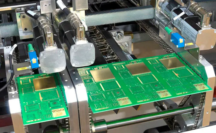
2. Component Placement
After solder paste application, components are placed onto their designated locations. Modern SMT lines use high-speed pick-and-place machines that can position components with remarkable accuracy (often within ±25 microns or better). These machines utilize advanced vision systems to align components with the PCB pads and can place tens of thousands of components per hour.
There are several types of placement machines:
- High-speed placers: Optimized for small, lightweight components like resistors and capacitors
- Multi-function placers: Capable of handling larger or irregularly shaped components
- Ultra-high accuracy placers: Used for fine-pitch components like micro-BGAs
3. Reflow Soldering
Once components are placed, the PCB moves through a reflow oven where carefully controlled temperature profiles melt the solder paste, creating permanent electrical and mechanical connections. The reflow profile typically consists of four zones:
- Preheat: Gradually raises the board temperature to activate flux and prevent thermal shock
- Soak: Allows temperature stabilization across the entire assembly
- Reflow: Exceeds the solder’s melting point to form proper intermetallic bonds
- Cooling: Solidifies the solder joints at a controlled rate
4. Inspection and Testing
Post-reflow inspection is essential for quality control. Common inspection methods include:
- Automated Optical Inspection (AOI): Uses cameras to verify component presence, placement accuracy, and solder joint quality
- X-ray Inspection: Essential for examining hidden joints like those in BGA packages
- In-Circuit Testing (ICT): Electrical verification of component values and circuit functionality
- Functional Testing: Validates the complete assembly’s operation
5. Cleaning (if required)
While many modern solder pastes are “no-clean” formulations, some applications may require post-assembly cleaning to remove flux residues, particularly for high-reliability products or when conformal coating will be applied.
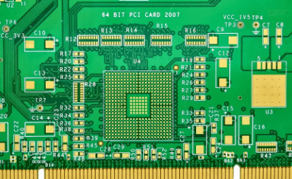
SMT Components and Packaging
SMT components come in standardized package sizes and forms, designed for machine handling and placement. Common package types include:
- Passive Components:
- Resistors, capacitors, and inductors typically use rectangular chip packages (e.g., 0201, 0402, 0603, 0805, 1206), where the numbers represent dimensions in hundredths of an inch (e.g., 0402 = 0.04″ × 0.02″)
- Integrated Circuits:
- Small Outline Transistor (SOT) packages
- Small Outline Integrated Circuit (SOIC)
- Quad Flat Packages (QFP)
- Ball Grid Arrays (BGA)
- Chip Scale Packages (CSP)
- Wafer-Level Chip Scale Packages (WLCSP)
- Discrete Semiconductors:
- Diodes in SOD packages
- Transistors in SOT packages
The trend in SMT component development has been toward ever-smaller packages to enable higher circuit density and miniaturization. This has led to the creation of microscopic components like the 01005 (0.4mm × 0.2mm) and even smaller metric sizes for specialized applications.
Advantages of SMT Patch Technology
SMT offers numerous benefits over traditional through-hole technology:
- Miniaturization: SMT components are significantly smaller than their through-hole counterparts, allowing for higher circuit density and smaller end products.
- Improved Performance: Shorter lead lengths reduce parasitic inductance and capacitance, enabling better high-frequency performance.
- Automation Compatibility: SMT components are designed for machine placement, enabling high-volume automated production with minimal human intervention.
- Cost Efficiency: While setup costs can be high, per-unit costs are lower at scale due to faster production speeds and reduced material usage.
- Dual-Side Assembly: PCBs can be populated on both sides, further increasing density and reducing size.
- Mechanical Reliability: Surface mount joints are less prone to failure from vibration and mechanical shock compared to through-hole leads.
- Reduced Drilling: Eliminates the need for most through-holes, simplifying PCB fabrication.
Challenges in SMT Implementation
Despite its advantages, SMT presents several technical challenges:
- Thermal Management: Small components have limited thermal mass, making them susceptible to thermal shock during soldering.
- Component Handling: Miniature components require careful handling and storage to prevent damage or loss.
- Inspection Difficulty: Some solder joints (particularly under BGA components) are not visible, requiring specialized inspection methods.
- Rework Complexity: Repairing or replacing SMT components often requires specialized tools and skills.
- Thermal Expansion Mismatch: Differences in thermal expansion coefficients between components and PCB can lead to stress on solder joints.
- Electrostatic Discharge (ESD) Sensitivity: Many SMT components are highly sensitive to ESD, requiring strict handling protocols.
Future Trends in SMT Technology
The SMT industry continues to evolve, with several notable trends shaping its future:
- Advanced Miniaturization: The push for smaller components continues, with 008004 packages (0.25mm × 0.125mm) and wafer-level packaging gaining traction.
- High-Density Interconnect (HDI): Combining SMT with microvias and finer trace widths enables even greater circuit density.
- 3D Packaging: Technologies like Package-on-Package (PoP) and Through-Silicon Vias (TSV) allow vertical integration of components.
- Advanced Materials: New substrate materials and low-temperature solder alloys address challenges in flexible electronics and high-reliability applications.
- Smart Manufacturing: Integration of Industry 4.0 concepts, including IoT-enabled equipment, AI-based process optimization, and predictive maintenance.
- Heterogeneous Integration: Combining SMT with other assembly technologies to integrate diverse components (e.g., MEMS, optical devices) on single substrates.
- Environmental Considerations: Development of lead-free, halogen-free, and low-energy processes to meet environmental regulations.
Quality Control in SMT Patch
Maintaining high quality in SMT assembly requires comprehensive process control:
- Solder Paste Management: Proper storage, handling, and application of solder paste to prevent defects.
- Stencil Design Optimization: Aperture size and shape significantly impact paste deposition quality.
- Placement Accuracy: Regular calibration of placement machines to maintain precision.
- Reflow Profile Optimization: Tailoring temperature profiles to specific assemblies and components.
- Statistical Process Control (SPC): Monitoring key parameters to detect and correct process drift.
- Failure Analysis: Systematic investigation of defects to identify root causes and implement corrective actions.
Conclusion
SMT patch technology has become the backbone of modern electronics manufacturing, enabling the production of increasingly sophisticated and compact electronic devices that power our digital world. From smartphones and computers to medical devices and automotive systems, SMT’s influence is ubiquitous.
As the technology continues to advance, manufacturers face both opportunities and challenges in implementing SMT processes that can keep pace with the demands for higher density, improved performance, and greater reliability. The future of SMT will likely see further integration with other advanced packaging technologies, creating hybrid assembly approaches that push the boundaries of what’s possible in electronics manufacturing.
Understanding the principles, processes, and challenges of SMT patch technology is essential for anyone involved in electronics design, manufacturing, or quality assurance. As component sizes shrink and performance requirements grow, the importance of optimized SMT processes will only increase, making ongoing education and process refinement critical for success in this field.