Custom Circuit Board Assembly: Advanced Methods for Modern Manufacturing
Key Takeaways
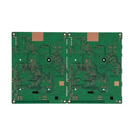
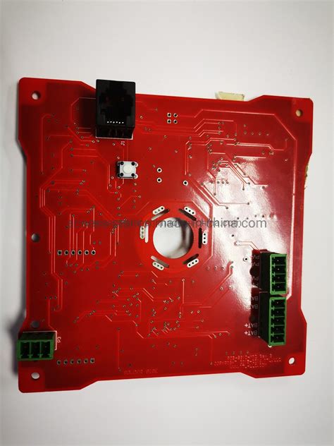
Modern PCB assembly relies on precision engineering to ensure components meet exact design specifications, particularly in PCBA workflows where accuracy directly impacts performance. Streamlined production methods, such as automated pick-and-place systems and reflow soldering, reduce assembly time while maintaining consistency. Innovations in quality control, including automated optical inspection (AOI) and X-ray testing, are critical for identifying defects in high-density boards.
"Adopting scalable PCB assembly solutions allows manufacturers to balance customization with volume demands, ensuring adaptability across industries like automotive and IoT."
For PCBA projects, integrating design-for-manufacturing (DFM) principles early minimizes rework and accelerates time-to-market. Advanced techniques like laser depaneling and 3D solder paste inspection further enhance reliability in complex layouts. To optimize efficiency, consider pairing real-time process monitoring with modular assembly lines, enabling rapid adjustments for evolving technical requirements.
Precision Engineering in PCB Manufacturing
Modern PCB assembly relies on precision engineering to meet the exacting demands of today’s electronics. At the core of PCBA (Printed Circuit Board Assembly) lies the integration of nanometer-scale components and multilayer substrates, which require advanced manufacturing tools to ensure accuracy. Laser-guided placement systems, for instance, achieve tolerances under 10 microns, minimizing errors in high-density interconnect (HDI) designs.
Contemporary techniques like automated optical inspection (AOI) and 3D solder paste monitoring further enhance precision by detecting defects in real time. This approach ensures consistent quality, particularly in applications such as medical devices or aerospace systems, where reliability is non-negotiable. Engineers also prioritize material selection, opting for low-loss dielectrics and high-temperature laminates to maintain performance under stress.
A critical aspect of precision engineering involves scalable PCB integration, balancing speed with meticulous attention to detail. Thermal management strategies, including controlled impedance routing and embedded cooling channels, address heat dissipation challenges in compact designs. By leveraging advanced manufacturing methods, such as robotic soldering and AI-driven process optimization, PCBA workflows achieve repeatability while adapting to evolving product specifications.
This precision extends beyond hardware, incorporating design-for-manufacturing (DFM) principles to streamline collaboration between design teams and assembly facilities. Manufacturers that master these methodologies consistently deliver custom circuit board assemblies capable of powering next-generation technologies.
Streamlined Production for PCB Integration
Efficient integration of PCB assembly (PCBA) into modern manufacturing relies on optimized workflows that minimize bottlenecks while maintaining precision. Central to this effort is the adoption of automated assembly lines, which reduce manual intervention and accelerate throughput. By implementing surface-mount technology (SMT) alongside automated optical inspection (AOI), manufacturers achieve consistent placement accuracy and detect defects in real time, ensuring seamless integration with downstream processes.
Key aspects of streamlined PCBA production include:
| Traditional Methods | Streamlined Approaches |
|---|---|
| Manual component placement | Robotic pick-and-place systems |
| Post-production quality checks | In-line AOI verification |
| Disjointed supply chain coordination | Integrated ERP systems |
| 4–6 week lead times | 2–3 week rapid turnaround |
Another critical element is design-for-manufacturability (DFM) analysis, which identifies potential production challenges during the prototyping phase. This proactive approach reduces rework by 40–60% in complex PCB assembly projects. Additionally, just-in-time (JIT) material management synchronizes component delivery with production schedules, cutting inventory costs by up to 30%.
By unifying these strategies, manufacturers achieve scalable PCB integration capable of supporting both low-volume prototyping and high-volume runs. The result is a 25–50% improvement in time-to-market for custom PCBA solutions across industries ranging from IoT devices to industrial automation.
Quality Control Innovations in Circuit Assembly
Modern PCB assembly processes demand rigorous quality assurance to meet evolving industry standards. Innovations in inspection technologies, such as automated optical inspection (AOI) and AI-powered defect detection, now enable real-time identification of soldering flaws, component misalignment, and trace irregularities. By integrating machine learning algorithms into PCBA workflows, manufacturers can predict failure patterns and optimize calibration parameters before production begins, reducing rework rates by up to 40%.
Advanced statistical process control (SPC) systems further enhance consistency, tracking variables like solder paste viscosity and reflow oven temperatures across batches. For high-density designs, 3D X-ray inspection provides non-destructive analysis of hidden connections, ensuring reliability in applications ranging from medical devices to aerospace systems. Additionally, blockchain-enabled traceability platforms are gaining traction, offering immutable records of material sourcing and testing outcomes.
These advancements align with the broader shift toward smart manufacturing, where IoT-enabled sensors monitor assembly lines for deviations, triggering automatic adjustments. Such innovations not only minimize human error but also support compliance with IPC-A-610 and ISO 9001 standards, critical for industries requiring zero-defect outputs. By prioritizing precision and scalability, these quality control methods ensure custom circuit board assembly meets both performance benchmarks and cost-efficiency targets.
Scalable Solutions for Modern PCB Assembly
Modern manufacturing demands require PCB assembly processes to adapt seamlessly to fluctuating production volumes while maintaining precision. Scalable solutions leverage modular design frameworks and automated workflows to accommodate both prototyping and high-volume runs. By integrating PCBA platforms with smart factory systems, manufacturers gain real-time data analytics to optimize throughput and resource allocation. For instance, configurable assembly lines enable rapid reconfiguration for different board complexities, reducing downtime during product transitions.
A key innovation lies in cloud-based inventory management, which synchronizes component procurement with production schedules, minimizing delays caused by supply chain disruptions. Advanced PCB assembly providers also employ predictive maintenance algorithms to preempt equipment failures, ensuring uninterrupted operations during scale-up phases. Additionally, standardized testing protocols embedded within scalable workflows guarantee consistent quality across batches, even as output increases.
To address evolving IoT and AI-driven applications, scalable PCBA systems now prioritize compatibility with embedded sensors and edge-computing modules. This approach not only future-proofs manufacturing setups but also streamlines integration with downstream smart devices. By balancing flexibility with robust process controls, scalable solutions empower manufacturers to meet dynamic market demands without sacrificing reliability or cost-efficiency.
Advanced Manufacturing Methods for PCBs
Modern PCB assembly relies on innovative techniques to meet the demands of high-performance electronics. Central to this evolution is the adoption of automated optical inspection (AOI) systems, which enhance accuracy by detecting microscopic defects in real time. Combined with PCBA-optimized pick-and-place robotics, manufacturers achieve precise component alignment, even for ultra-fine-pitch designs.
Another breakthrough involves additive manufacturing for prototyping, allowing rapid iteration of complex custom circuit board assembly projects. Laser-direct imaging (LDI) further refines circuit patterning, reducing etch times while improving trace resolution. For high-volume production, modular assembly lines integrate adaptive soldering technologies, such as vacuum reflow ovens, to minimize thermal stress on sensitive components.
To address scalability, advanced PCB assembly workflows now incorporate machine learning algorithms for predictive maintenance, reducing downtime. Meanwhile, embedded component packaging streamlines PCBA by integrating passive elements directly into substrate layers, optimizing space and signal integrity. These methods collectively support tighter tolerances required for applications like IoT devices and automotive systems, ensuring both efficiency and reliability align with modern manufacturing standards.
Cutting-Edge Circuit Board Assembly Processes
Modern PCB assembly relies on innovative methodologies to meet the demands of high-performance electronics. Central to these advancements is the integration of automated optical inspection (AOI) systems, which enable real-time defect detection during PCBA workflows. By combining machine vision algorithms with high-resolution imaging, manufacturers achieve micron-level accuracy in component placement, significantly reducing rework rates.
Another breakthrough lies in laser-assisted soldering, which ensures precise thermal control for delicate components, particularly in high-density interconnect (HDI) designs. This technique minimizes thermal stress while maintaining robust electrical connections—a critical factor for aerospace and medical devices requiring PCB assembly reliability.
Emerging additive manufacturing techniques are also reshaping PCBA processes, allowing for rapid prototyping of complex circuit geometries. Hybrid approaches that merge 3D-printed substrates with traditional surface-mount technology (SMT) create opportunities for lightweight, compact designs without compromising functionality.
To further enhance scalability, manufacturers are adopting modular assembly lines equipped with IoT-enabled sensors. These systems collect performance data across production stages, enabling predictive maintenance and dynamic process optimization. Such innovations not only accelerate throughput but also align with evolving industry standards for energy efficiency and material sustainability in PCB assembly.
By leveraging these cutting-edge methods, the industry continues to push the boundaries of what’s achievable in precision, speed, and adaptability for modern electronics manufacturing.
Optimizing Efficiency in Custom PCB Assembly
Achieving peak efficiency in PCB assembly requires a strategic balance between design optimization and process automation. Modern manufacturers leverage PCBA-specific tools like real-time monitoring systems to identify bottlenecks in solder paste application or component placement. By integrating design for manufacturability (DFM) checks early in the prototyping phase, teams can reduce rework cycles by up to 30%, ensuring smoother transitions to full-scale production.
Advanced automated optical inspection (AOI) systems now use machine learning algorithms to detect microscopic defects in high-density interconnect (HDI) boards, slashing inspection times by 40% compared to manual methods. For mixed-technology assemblies, combining surface-mount technology (SMT) with selective soldering streamlines workflows while maintaining precision in complex layouts.
Scalability is further enhanced through modular PCB assembly lines, where reconfigurable robotic arms adapt to varying batch sizes without downtime. Energy-efficient curing ovens and dynamic thermal profiling tools also minimize material waste, aligning with lean manufacturing principles. By embedding IoT sensors in PCBA testing stations, manufacturers gain predictive insights into equipment maintenance needs, preventing unplanned stoppages.
These innovations not only accelerate time-to-market but ensure consistent quality across high-mix, low-volume production runs—a critical advantage in industries demanding rapid customization.
Custom Circuit Board Assembly Techniques
Modern PCB assembly relies on a blend of precision engineering and adaptive manufacturing strategies to meet diverse industry demands. Central to this process is surface-mount technology (SMT), which enables high-density component placement on compact PCBA designs. By combining automated pick-and-place systems with laser-aligned soldering, manufacturers achieve micron-level accuracy, critical for applications like IoT devices and medical electronics.
Advanced manufacturing methods now prioritize design for manufacturability (DFM) principles, ensuring layouts are optimized for both performance and cost-effective scaling. For instance, thermal management considerations during the PCB assembly phase reduce failure risks in high-power circuits, while automated optical inspection (AOI) systems validate solder joint integrity across thousands of connections per hour.
Furthermore, hybrid approaches integrating through-hole technology (THT) with SMT allow flexibility in prototyping and low-volume PCBA runs. Techniques such as selective soldering minimize heat exposure for sensitive components, preserving functionality in harsh environments. The rise of modular assembly lines also supports rapid reconfiguration, enabling seamless transitions between product variants without compromising throughput.
By leveraging these evolving PCB assembly techniques, manufacturers balance precision, scalability, and adaptability—key factors in maintaining competitiveness across aerospace, automotive, and consumer electronics sectors. The integration of real-time analytics into assembly workflows further refines process control, ensuring consistent quality even as design complexities escalate.
Conclusion
The evolution of PCB assembly (PCBA) underscores its critical role in enabling modern manufacturing agility. By integrating precision engineering with streamlined production workflows, manufacturers can address the growing demand for specialized electronics while maintaining rigorous quality control standards. Innovations such as automated optical inspection (AOI) and AI-driven defect detection have elevated reliability in custom circuit board assembly, ensuring compliance with industry benchmarks even at high volumes.
Scalability remains a cornerstone of contemporary PCB integration, with modular design frameworks allowing seamless adaptation to diverse applications—from IoT devices to industrial automation. The shift toward data-driven manufacturing further optimizes material usage and reduces waste, aligning with sustainability goals without compromising efficiency. As advanced manufacturing methods continue to refine PCBA processes, the focus on rapid prototyping and flexible supply chains will empower businesses to respond dynamically to market shifts. By prioritizing both technical excellence and operational adaptability, the future of custom circuit board assembly promises to bridge innovation with practical, large-scale implementation.
FAQs
What distinguishes custom PCB assembly from standard assembly processes?
Custom PCB assembly focuses on tailoring design specifications, component selection, and manufacturing workflows to meet unique application requirements. Unlike standardized methods, it integrates advanced techniques like laser-drilled vias and high-density interconnects to optimize performance for specialized industries.
How do manufacturers ensure quality in PCBA workflows?
Modern PCBA processes employ automated optical inspection (AOI), X-ray testing, and in-circuit testing to detect defects at micron-level precision. These innovations align with ISO 9001 standards, ensuring reliability across aerospace, medical, and IoT applications.
Can PCB assembly scale for high-volume production without compromising precision?
Yes, scalable PCB assembly solutions combine modular production lines with real-time data analytics. This allows manufacturers to adjust throughput dynamically while maintaining ±0.002" placement tolerances and <1% defect rates, even for batches exceeding 100,000 units.
What role does PCBA play in accelerating product development cycles?
By leveraging rapid prototyping and design-for-manufacturability (DFM) analysis, PCBA services reduce lead times by up to 40%. This agility supports iterative testing, enabling faster transitions from concept validation to full-scale production.
Are there eco-friendly options for custom PCB assembly?
Leading providers now offer halogen-free substrates and lead-free soldering techniques, complying with RoHS and REACH directives. These sustainable practices minimize environmental impact while maintaining thermal stability and signal integrity.
Ready to Optimize Your PCB Assembly Workflow?
For tailored solutions in PCBA design and manufacturing, please click here to explore advanced engineering capabilities and request a project consultation.