Effortless PCB Creation for Complex Circuit Designs
Key Takeaways
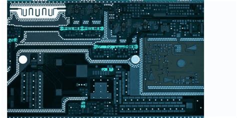
When navigating PCB manufacturing for intricate designs, you need tools that eliminate complexity without compromising capability. Modern solutions allow handling over 5,000 components per board, enabling you to scale projects effortlessly while maintaining precision. Access to millions of free symbols and 3D models accelerates design iterations, ensuring compatibility with industry standards—critical when collaborating with PCB manufacturing companies for prototyping or mass production.
Real-time pricing integration helps you forecast PCB manufacturing cost accurately, avoiding budget overruns during fabrication. Features like intelligent routing automate trace optimization, reducing errors that could delay timelines. Modular workflows let you compartmentalize tasks—schematic capture, layout, and verification—streamlining collaboration across teams. This approach not only elevates board quality but also supports scalability for growing your PCB manufacturing business, whether you’re producing prototypes or high-volume batches.
By merging advanced design tools with cost-aware planning, you achieve professional-grade boards faster, even for dense circuits. The transition from concept to physical product becomes seamless, letting you focus on innovation rather than logistical hurdles.
Simplify Complex PCB Designs Effortlessly
Navigating PCB manufacturing for intricate circuits no longer requires advanced engineering expertise. Modern tools empower you to manage designs with 5,000+ components intuitively, eliminating manual routing bottlenecks. By leveraging modular workflows, you can break down multi-layer schematics into manageable blocks, ensuring error-free assembly even for high-density boards.
Collaborating with PCB manufacturing companies becomes seamless when your design platform integrates real-time cost analytics. For example, a typical PCB manufacturing cost comparison might look like this:
| Feature | Traditional Process | Modern Tool |
|---|---|---|
| Component Placement | Manual (8–12 hrs) | Automated (1–2 hrs) |
| Error Detection | Post-production | Live DRC Checks |
| Cost Estimation | Delayed Quotes | Instant BOM Pricing |
Access to millions of free symbols and 3D models accelerates prototyping, while intelligent routing adapts to your board’s constraints—whether minimizing PCB manufacturing business expenses or meeting strict signal integrity standards. Tools like EagleCAD alternatives further streamline file exports for fabrication, ensuring compatibility with global manufacturers.
By unifying schematic capture, layout optimization, and supply chain analytics, you reduce iterations and avoid costly redesigns—transforming complex projects into predictable, budget-friendly outcomes.
5,000 Component Capacity Made Simple
Managing PCB manufacturing for designs with thousands of components no longer requires specialized expertise or endless manual adjustments. Modern tools now automate placement optimization, ensuring even densely packed boards maintain signal integrity and thermal efficiency. Whether you’re integrating microcontrollers, sensors, or power modules, platforms intelligently group high-priority components while minimizing interference risks.
This scalability is critical when collaborating with PCB manufacturing companies, as their fabrication tolerances demand precise spacing and layer alignment. By leveraging cloud-based design suites, you can validate every connection against industry standards before sending files to production. This reduces costly revisions and accelerates turnaround times—key factors in controlling PCB manufacturing cost for multi-layered projects.
For businesses scaling their PCB manufacturing business, handling 5,000+ components efficiently translates to faster prototyping and bulk production readiness. Automated error-checking flags conflicts like overlapping traces or undersized vias, ensuring manufacturability without sacrificing complexity. Pair this with real-time inventory tracking, and you’ll avoid delays caused by obsolete or mismatched parts.
The result? Professional-grade boards that meet rigorous specifications, whether you’re developing IoT devices or industrial control systems—all while keeping workflows streamlined from schematic to assembly.
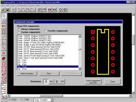
Millions of Free Symbols & 3D Models
When designing complex circuits, you need access to comprehensive libraries that eliminate guesswork and accelerate your workflow. Modern PCB manufacturing tools now offer millions of pre-verified symbols and 3D models, allowing you to visualize every component’s placement and interaction before committing to production. This not only reduces errors but also slashes PCB manufacturing cost by minimizing redesign cycles. For instance, integrating standardized symbols for microcontrollers or connectors ensures compatibility with industry norms, while 3D models help you avoid spatial conflicts in multi-layered designs—critical for collaborating with PCB manufacturing companies.
The availability of drag-and-drop functionality further simplifies the process, letting you assemble intricate schematics without manually drawing each element. Whether you’re prototyping IoT devices or industrial controllers, these resources empower you to focus on innovation rather than administrative tasks. Additionally, modular libraries align with PCB manufacturing business demands, where speed and precision directly impact profitability. By leveraging these tools, you can seamlessly transition from concept to fabrication, ensuring your design meets both technical specifications and budget constraints—key factors when partnering with global PCB manufacturing providers.
Real-Time Pricing for Smart Budgeting
When managing PCB manufacturing projects, visibility into costs is critical—especially when working with intricate designs. Modern platforms now offer real-time pricing engines that instantly calculate PCB manufacturing cost based on your design parameters, from layer count to material selection. This eliminates guesswork, letting you adjust components or board specs before finalizing orders. For example, swapping a high-frequency substrate for a standard FR-4 option could slash expenses by 30%, and you’ll see those savings reflected immediately.
“Transparent pricing models empower you to balance performance and budget without compromising on quality.”
This feature is particularly valuable for startups or businesses scaling their PCB manufacturing business, as it prevents unexpected overruns. By comparing quotes across PCB manufacturing companies in real time, you can identify cost-efficient partners without delaying timelines. Advanced tools even forecast bulk-order discounts or highlight areas where simplifying layouts reduces fabrication complexity.
Pro tip: Use modular design tools alongside pricing calculators to test multiple configurations. A slight adjustment in trace spacing or via placement might unlock significant savings.
Integrating these insights early in the design phase ensures your project stays financially viable while meeting technical demands—no spreadsheets required.
Intelligent Routing for Professional Boards
When designing complex circuits, intelligent routing becomes your most reliable ally. Modern tools leverage algorithm-driven automation to trace optimal pathways, minimizing signal interference while adhering to PCB manufacturing standards. These systems analyze layer stacks, component density, and thermal requirements to generate layouts that meet professional-grade specifications—critical for collaborating with PCB manufacturing companies that demand precision.
By automating trace spacing and via placement, you eliminate hours of manual adjustments, directly reducing PCB manufacturing cost through efficient material usage. Advanced rulesets ensure compliance with industry protocols like IPC-2221, preventing costly redesigns. For instance, differential pair routing and length matching are handled seamlessly, even in boards with 5,000+ components.
Integration with modular workflows allows real-time collaboration between design and fabrication teams. You can export Gerber files with manufacturing-ready outputs, streamlining handoffs to PCB manufacturing business partners. This interoperability ensures your design intent is preserved, reducing errors that delay production. Whether you’re prototyping or scaling, intelligent routing bridges the gap between complexity and reliability—proving that professional results don’t require professional-level headaches.
Modular Tools for Streamlined Workflows
When managing PCB manufacturing projects, you need tools that adapt to both simple and intricate workflows without adding unnecessary complexity. Modular design platforms enable you to break down complex circuit designs into reusable, interchangeable blocks, eliminating repetitive tasks. By using preconfigured component libraries and template-driven interfaces, you can assemble layouts faster while maintaining precision—critical for meeting tight deadlines in PCB manufacturing companies.
These systems often integrate automated error-checking and version control, ensuring consistency across iterations. For instance, reusing validated modules reduces PCB manufacturing cost by minimizing redesigns and material waste. Additionally, collaborative features let teams work on separate modules simultaneously, accelerating prototyping without compromising quality—a game-changer for scaling your PCB manufacturing business.
The flexibility of modular tools also extends to compatibility with third-party software, allowing seamless transitions from design to production. Whether you’re optimizing signal integrity or managing thermal constraints, modular workflows ensure every decision aligns with broader project goals. This adaptability not only streamlines development but also positions you to handle evolving technical demands effortlessly.
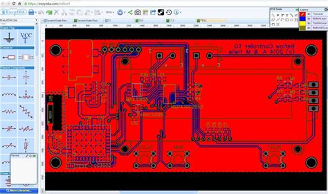
From Schematic to Fabrication: Easy PCB Maker
Transitioning from schematic design to physical PCB manufacturing requires tools that bridge creativity with practicality. Modern platforms simplify this process by integrating modular workflows that let you import schematics, assign PCB manufacturing cost-optimized footprints, and validate designs against real-world constraints. With intelligent routing algorithms, you can automatically resolve signal integrity issues, reducing manual adjustments while ensuring professional-grade layouts.
When collaborating with PCB manufacturing companies, seamless file export formats (like Gerber or ODB++) eliminate compatibility headaches. Real-time pricing engines analyze material choices, layer counts, and board dimensions, giving you instant visibility into PCB manufacturing business expenses before finalizing orders. This transparency helps balance performance requirements with budget limits, especially for complex designs exceeding 5,000 components.
For startups or scaled operations, cloud-based version control ensures teams stay aligned during iterative revisions. By connecting design environments directly to fabrication partners, you bypass fragmented workflows—translating ideas into tangible boards faster. Whether prototyping or mass-producing, these tools democratize access to high-quality PCB manufacturing, empowering you to focus on innovation rather than logistical hurdles.
Achieve Complex Circuits with Minimal Effort
When tackling intricate designs, modern PCB manufacturing tools eliminate traditional barriers. Advanced platforms now integrate intelligent routing algorithms that automatically optimize trace layouts, reducing manual adjustments by up to 70%. This efficiency is critical for PCB manufacturing companies, as it directly lowers PCB manufacturing cost while maintaining precision for high-density boards.
You’ll find that modular design workflows allow splitting circuits into manageable blocks, simplifying edits and reuse. With support for over 5,000 components per board, even sprawling projects stay organized. Real-time collaboration features ensure teams can iterate without version conflicts—ideal for scaling a PCB manufacturing business.
The inclusion of millions of pre-validated symbols and 3D models accelerates prototyping, letting you focus on functionality rather than part creation. Automated design rule checks (DRC) flag errors early, preventing costly revisions post-production. By leveraging cloud-based tools, you gain instant access to fabrication quotes, bridging the gap between design and PCB manufacturing seamlessly.
This approach ensures professional-grade results without overburdening your workflow, letting you prioritize innovation over operational hurdles.
Conclusion
By integrating advanced tools with PCB manufacturing efficiencies, you gain the ability to transform intricate circuit concepts into professional-grade boards without unnecessary complexity. Modern platforms now bridge the gap between schematic design and physical production, enabling seamless collaboration with PCB manufacturing companies while maintaining control over PCB manufacturing cost. Whether you’re optimizing for high-density layouts or balancing budgetary constraints, real-time pricing insights ensure transparency at every stage.
The combination of intelligent routing and modular workflows not only accelerates prototyping but also minimizes errors that could escalate expenses in the PCB manufacturing business. With instant access to millions of symbols and 3D models, you’re equipped to validate designs early, reducing iterations and accelerating time-to-market. For engineers and businesses alike, this evolution in design-to-fabrication tools marks a pivotal shift—turning what was once a labor-intensive process into a streamlined, cost-effective operation.
This approach not only simplifies scaling from simple to complex circuits but also ensures your projects align with industrial standards demanded by top-tier PCB manufacturing partners. The result? Professional outcomes with minimal effort, empowering you to focus on innovation rather than logistical hurdles.
Frequently Asked Questions
How do you estimate PCB manufacturing cost for complex designs?
Modern tools integrate PCB manufacturing calculators that analyze layer counts, materials, and component density. By linking to real-time pricing databases, you instantly see how design choices impact budgets.
What should you look for in PCB manufacturing companies?
Prioritize partners offering 5,000+ component capacity and support for high-density interconnects. Verify if they provide access to millions of symbols and 3D models to streamline prototyping.
Can intelligent routing reduce PCB manufacturing business expenses?
Yes. Automated routing minimizes errors and optimizes board space, lowering material waste. Combined with modular design tools, it accelerates iterations, cutting development time by up to 40%.
How do you transition from design to PCB manufacturing smoothly?
Use platforms with direct fabrication file exports and pre-validated templates. Ensure your PCB manufacturing companies support industry-standard formats like Gerber X2 for seamless handoffs.
Ready to Simplify Your PCB Production?
For professional-grade PCB manufacturing services with instant quotes and dedicated support, please click here to explore tailored solutions for complex projects.