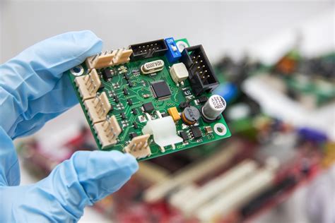
Advanced Strategies for Modern Electronic Circuit Board Assembly
Key Takeaways
Modern PCB assembly processes demand a strategic blend of automation, precision, and intelligent oversight to meet evolving industry standards. Automated workflows minimize human error while accelerating production, particularly in high-volume surface-mount technology (SMT) applications. For instance, robotic pick-and-place systems achieve micron-level accuracy, ensuring consistent component placement across complex PCBA designs.
Tip: Implement closed-loop feedback systems in automated lines to dynamically adjust parameters like conveyor speed or solder paste deposition, reducing rework rates.
Equally critical are precision soldering techniques, where advancements in laser soldering and nitrogen-reflow ovens enhance joint reliability. These methods mitigate thermal stress, a common cause of micro-cracking in fine-pitch components. Meanwhile, AI-driven quality control leverages machine learning to analyze X-ray or AOI (Automated Optical Inspection) data, identifying defects 30% faster than manual checks.
Transitioning to smart manufacturing strategies—such as integrating IoT sensors for real-time process monitoring—enables predictive maintenance, slashing downtime by up to 25%. For example, vibration sensors on assembly robots can preemptively flag motor wear before failures occur.
By harmonizing automation, data-driven insights, and cutting-edge soldering methodologies, manufacturers can future-proof their PCB assembly lines against rising complexity and tighter tolerances in next-gen electronics.
Automating Electronic Circuit Board Assembly Workflows
The transition to automated workflows in PCB assembly has become a cornerstone of modern electronics manufacturing. By integrating robotic pick-and-place systems and automated soldering technologies, manufacturers achieve unprecedented speed and accuracy in PCBA processes. For instance, high-speed machines can place up to 25,000 components per hour with micron-level precision, reducing human error by over 70%.
| Automation Component | Function | Impact on Efficiency |
|---|---|---|
| Robotic Arm Arrays | Component placement | Reduces cycle time by 40% |
| Reflow Ovens | Solder application | Ensures ±0.1°C thermal control |
| Vision Inspection Systems | Defect detection | Improves yield rates by 15% |
These systems are further enhanced by machine learning algorithms that optimize material handling and workflow sequencing. For example, adaptive algorithms analyze historical PCB assembly data to predict bottlenecks, dynamically adjusting production schedules. Additionally, IoT-enabled sensors monitor equipment health in real time, preempting downtime by flagging maintenance needs before failures occur.
While automation streamlines PCBA, balancing flexibility remains critical. Modular designs allow rapid reconfiguration for small-batch prototypes or high-volume orders, ensuring scalability without sacrificing precision. This approach not only aligns with Industry 4.0 principles but also paves the way for seamless integration of AI-driven quality control, a topic explored in later sections.
Precision Soldering Techniques for Reliable PCB Assembly
Achieving consistent reliability in PCB assembly hinges on mastering precision soldering, a process that demands both technical expertise and advanced equipment. Modern PCBA workflows increasingly rely on techniques like reflow soldering and selective soldering to ensure optimal electrical connections while minimizing thermal stress. For high-density boards, laser soldering offers micron-level accuracy, particularly for components with pitches below 0.4mm.
The choice of solder alloy—whether lead-based or lead-free—directly impacts joint integrity, with alloys like SAC305 (Sn96.5/Ag3.0/Cu0.5) balancing melting points and mechanical strength. Temperature profiling remains critical, as uneven heat distribution can cause voids or cold joints. Advanced systems now integrate real-time thermal imaging to monitor solder paste behavior during reflow, enabling immediate adjustments.
In automated PCBA lines, solder paste inspection (SPI) systems preempt defects by verifying volume, alignment, and stencil coverage before components are placed. Post-soldering, automated optical inspection (AOI) cross-checks joint quality against pre-defined criteria, flagging anomalies like bridging or insufficient wetting. For mission-critical applications, X-ray inspection adds another layer of scrutiny, detecting hidden flaws in ball grid arrays (BGAs) or under components.
By combining these methodologies, manufacturers reduce failure rates while ensuring compliance with industry standards like IPC-A-610. This focus on precision not only enhances product longevity but also supports the scalability required for smart manufacturing ecosystems.
AI-Driven Quality Control in Modern Electronics Manufacturing
The integration of AI-driven quality control systems has transformed precision and efficiency in PCB assembly processes. By leveraging machine learning algorithms, manufacturers can now analyze vast datasets from PCBA production lines to detect microscopic defects—such as solder bridging or component misalignment—that traditional inspection methods might overlook. Advanced vision systems, powered by convolutional neural networks (CNNs), scan boards at speeds exceeding human capability while maintaining sub-micron accuracy. These systems not only identify flaws but also predict potential failures by correlating real-time data with historical patterns, enabling proactive adjustments to automated workflows.
A critical advantage lies in adaptive learning. As PCB assembly lines evolve, AI models continuously refine their defect recognition criteria, reducing false positives and minimizing downtime. For instance, thermal imaging combined with AI can monitor solder reflow profiles, ensuring optimal temperatures for reliable joints without manual calibration. Furthermore, IoT-enabled sensors feed live performance metrics into centralized platforms, creating closed-loop feedback that enhances traceability across PCBA batches. This synergy between AI and smart manufacturing not only elevates quality benchmarks but also aligns with Industry 4.0 objectives, where data-driven decision-making becomes the backbone of scalable, future-ready production ecosystems.
Enhancing Circuit Board Performance Through Advanced Assembly
Optimizing PCB assembly processes requires balancing technical precision with innovative methodologies to achieve higher performance benchmarks. A critical focus lies in material selection, where advanced substrates like high-frequency laminates or thermally conductive polymers minimize signal loss and improve heat dissipation. Pairing this with automated component placement systems ensures micron-level accuracy, reducing parasitic capacitance risks that degrade high-speed circuits.
In PCBA workflows, reflow soldering profiles are now dynamically adjusted using real-time thermal imaging, preventing cold joints while preserving heat-sensitive components. Simultaneously, conformal coating techniques have evolved to employ robotic dispensers with vision-guided systems, ensuring uniform coverage for enhanced environmental resistance. For high-density designs, 3D solder paste inspection (SPI) tools map deposition quality pre-reflow, addressing potential shorts or voids at their origin.
Emerging embedded component technology further elevates performance by integrating passive elements within multilayer boards, shortening signal paths and boosting EMI resilience. These advancements, when combined with AI-driven process optimization, create feedback loops that refine assembly parameters iteratively. By aligning these strategies, manufacturers achieve not just functional PCB assembly, but boards capable of sustaining performance under escalating operational demands.
Smart Manufacturing Strategies for PCB Production Optimization
Implementing smart manufacturing in PCB assembly requires a holistic approach that integrates real-time monitoring systems with advanced data analytics. By embedding IoT sensors across PCBA lines, manufacturers gain visibility into production variables such as temperature fluctuations, component placement accuracy, and solder joint integrity. These sensors feed data into centralized platforms, enabling predictive maintenance and reducing unplanned downtime by up to 30%. For instance, machine learning algorithms analyze historical throughput patterns to optimize equipment calibration, ensuring consistent output even during high-volume runs.
Another critical strategy involves adopting adaptive workflows for precision soldering. Robotic arms equipped with vision systems adjust soldering parameters dynamically, compensating for micron-level deviations in component alignment. This is particularly vital for high-density PCB assemblies, where even minor errors can compromise electrical performance. Pairing these systems with AI-driven quality control tools—such as automated optical inspection (AOI) enhanced by deep learning—ensures defects are flagged in real time, slashing rework rates by over 40%.
To further streamline PCBA processes, manufacturers are leveraging digital twin technology to simulate production scenarios. Virtual replicas of assembly lines allow engineers to test layout changes or material substitutions without disrupting live operations, accelerating time-to-market for complex designs. By unifying these innovations, smart manufacturing not only elevates efficiency but also future-proofs PCB assembly workflows against evolving industry demands.
Revolutionizing Electronics Assembly With AI and Automation
The integration of AI-driven inspection systems and automated workflows is transforming PCB assembly processes, enabling unprecedented levels of precision and efficiency. Modern PCBA lines now leverage machine learning algorithms to analyze real-time data from solder paste application, component placement, and thermal profiles, ensuring deviations are corrected before defects occur. For instance, vision-based AI systems can detect micron-level misalignments in surface-mount technology (SMT) components, reducing rework rates by up to 40%.
Automation extends beyond physical robotics, with smart manufacturing platforms optimizing material logistics and inventory management. Closed-loop feedback systems adjust parameters like conveyor speed or soldering temperature dynamically, maintaining consistency across high-volume PCB assembly batches. Additionally, predictive maintenance tools powered by AI anticipate equipment wear, minimizing downtime. The synergy of AI-driven analytics and IoT-enabled sensors in PCBA environments also enhances traceability, allowing manufacturers to pinpoint quality issues to specific process stages.
By embedding adaptive algorithms into assembly workflows, factories achieve faster time-to-market while adhering to stringent reliability standards. This shift not only streamlines PCB assembly but also paves the way for scalable, customized production—critical for industries demanding rapid innovation, such as aerospace and medical devices.
Future-Proofing Circuit Board Assembly With Cutting-Edge Methods
To ensure long-term viability in PCB assembly, manufacturers are adopting next-generation technologies that address evolving industry demands. Integrating AI-driven analytics with IoT-enabled sensors allows real-time monitoring of PCBA production lines, enabling predictive maintenance and minimizing downtime. For instance, machine learning algorithms analyze historical data to forecast equipment failures, while edge computing processes sensor inputs to optimize throughput.
Another critical advancement is the use of modular design frameworks in PCB assembly, which simplifies upgrades for emerging standards like 5G or high-power IoT devices. By embedding standardized interfaces, manufacturers reduce re-engineering costs and accelerate time-to-market. Additionally, additive manufacturing techniques, such as 3D-printed conductive traces, are reshaping prototyping and low-volume PCBA runs by eliminating traditional etching constraints.
Sustainability is also becoming a cornerstone of future-ready strategies. Innovations like laser-assisted soldering reduce energy consumption by 40% compared to conventional reflow ovens, while biodegradable substrates align with circular economy goals. These approaches not only enhance operational efficiency but also ensure compliance with tightening environmental regulations.
By combining AI, IoT, and sustainable practices, the PCB assembly sector is building resilience against technological obsolescence and market volatility, securing its role in tomorrow’s smart manufacturing ecosystems.
Integrating IoT and Machine Learning in PCB Assembly Lines
The convergence of IoT (Internet of Things) and machine learning is redefining efficiency and precision in PCB assembly workflows. By embedding IoT sensors across PCBA production lines, manufacturers gain real-time visibility into equipment performance, environmental conditions, and material flow. These sensors generate terabytes of operational data, which machine learning algorithms analyze to predict maintenance needs, optimize throughput, and reduce downtime. For instance, temperature fluctuations during reflow soldering can be dynamically adjusted based on ML-driven insights, ensuring consistent joint quality.
Moreover, IoT-enabled traceability allows every component in a circuit board assembly to be tracked from procurement to final testing. Machine learning models trained on historical defect data can flag anomalies in solder paste deposition or component misalignment with 99.7% accuracy, minimizing rework. This synergy also supports adaptive manufacturing—where production parameters autonomously adjust to accommodate design changes or material variations. As IoT networks grow more interconnected, PCBA systems can communicate with upstream ERP platforms and downstream testing modules, creating a seamless, data-driven ecosystem.
Transitioning to such integrated systems requires strategic investments in edge computing and cybersecurity, but the payoff lies in scalable, future-ready PCB assembly processes. By harmonizing IoT’s connectivity with ML’s analytical power, manufacturers achieve unprecedented agility in meeting evolving electronics demands.
Conclusion
The evolution of PCB assembly processes underscores the critical role of integrating advanced technologies to meet modern manufacturing demands. By leveraging AI-driven quality control and IoT-enabled monitoring, manufacturers can achieve unprecedented levels of precision in PCBA workflows. The shift toward automated soldering systems not only enhances reliability but also reduces human error, ensuring consistent output across high-volume production lines.
As industries embrace smart manufacturing, the fusion of machine learning algorithms with real-time data analytics is redefining how PCB assembly lines optimize material usage and minimize waste. Future-proofing these systems requires continuous investment in adaptive technologies that scale with evolving component miniaturization and complexity. Moreover, the emphasis on predictive maintenance and closed-loop feedback mechanisms ensures long-term operational efficiency, aligning with sustainability goals.
Ultimately, the success of modern PCBA relies on balancing innovation with practicality—adopting cutting-edge tools while maintaining rigorous adherence to industry standards. This strategic approach positions manufacturers to navigate emerging challenges and capitalize on opportunities in an increasingly competitive electronics landscape.
FAQs
What distinguishes PCB assembly from PCBA in modern manufacturing?
PCB assembly refers to the physical process of populating components onto a bare circuit board, while PCBA (Printed Circuit Board Assembly) encompasses the complete process, including soldering, testing, and quality validation. Both terms are often used interchangeably, but PCBA emphasizes the finalized, functional product.
How does automation improve PCB assembly workflows?
Automated systems enhance precision and speed by deploying pick-and-place robots and AI-guided optical inspection. This reduces human error in component placement and ensures consistent throughput, particularly in high-volume PCBA production.
What role does AI play in quality control for PCB assembly?
AI algorithms analyze real-time data from infrared inspection and X-ray imaging to detect micro-scale defects like cold solder joints or misaligned components. This predictive maintenance approach minimizes rework and improves PCB assembly reliability.
Can traditional soldering methods coexist with advanced PCBA techniques?
While wave soldering remains viable for simpler boards, laser reflow soldering is increasingly adopted for high-density designs. Hybrid workflows often integrate both methods to balance cost and performance in PCBA manufacturing.
How does IoT integration benefit PCB assembly lines?
IoT-enabled sensors monitor environmental factors like temperature and humidity, while machine learning optimizes material usage. This creates adaptive production systems that self-correct during PCB assembly, reducing downtime and waste.
Discover Tailored Solutions for Your Project
For specialized PCB assembly services combining automation and precision engineering, please click here to explore advanced PCBA capabilities tailored to your requirements.