Turnkey PCB Electronics: Precision Engineering for Scalable Production
Key Takeaways
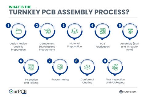
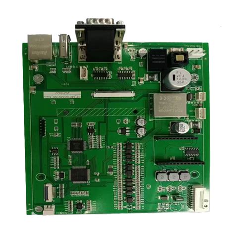
Effective PCB assembly relies on seamless integration of design, prototyping, and manufacturing. A turnkey PCB electronics approach ensures end-to-end oversight, minimizing delays and errors while optimizing cost efficiency and scalability. By consolidating workflows—from schematic design to PCBA (printed circuit board assembly)—manufacturers reduce supply chain fragmentation, enabling faster time-to-market.
Tip: Prioritize partners offering design-for-manufacturability (DFM) analysis during prototyping to identify potential production bottlenecks early.
Critical to scalable production is precision engineering, which guarantees consistent quality across high-volume runs. Advanced PCB assembly techniques, such as automated optical inspection (AOI) and surface-mount technology (SMT), ensure reliability in industries ranging from automotive to IoT. Additionally, modular PCBA designs allow flexible adaptation to evolving technical requirements, supporting cross-industry applications without retooling costs.
By aligning prototyping phases with mass production goals, teams can validate performance under real-world conditions while maintaining cost control. This holistic approach not only streamlines workflows but also strengthens quality assurance protocols, ensuring compliance with international standards like IPC-A-610.
Turnkey PCB Electronics Solutions
Modern electronics manufacturing demands seamless integration of design, prototyping, and production to meet evolving market needs. Turnkey PCB electronics solutions address this by offering end-to-end services that unify PCB assembly (PCBA) workflows, from schematic design to final product testing. By consolidating design validation, component sourcing, and PCBA processes under a single provider, businesses eliminate logistical bottlenecks while accelerating time-to-market.
A robust turnkey approach emphasizes precision engineering, ensuring that each PCB assembly stage adheres to industry standards for signal integrity, thermal management, and mechanical durability. Advanced manufacturers leverage automated optical inspection (AOI) and functional testing protocols to maintain consistency across low-volume prototypes and high-volume runs. This holistic strategy not only reduces material waste but also optimizes scalability—critical for industries transitioning from pilot programs to mass production.
Furthermore, turnkey partners often provide design-for-manufacturability (DFM) analysis, identifying potential flaws in board layouts before PCBA begins. Such proactive measures minimize costly redesigns and enhance yield rates. Whether serving automotive, medical, or IoT sectors, these integrated solutions ensure that every phase—from initial concept to final assembly—aligns with stringent quality benchmarks and cost-efficiency goals.
From Design to Volume Manufacturing
Transitioning from conceptual design to high-volume manufacturing requires seamless integration of PCB assembly (PCBA) processes with rigorous engineering protocols. Modern turnkey solutions bridge this gap by synchronizing design validation, prototyping, and scalability testing into a unified workflow. At the prototyping stage, engineers leverage automated design-for-manufacturability (DFM) tools to identify potential bottlenecks, such as component misalignment or thermal inefficiencies, ensuring designs are optimized for cost-efficient PCBA at scale.
A critical success factor lies in selecting materials and components that meet both performance criteria and volume production demands. For instance, surface-mount technology (SMT) enables rapid placement of microcomponents, while advanced inspection systems like automated optical inspection (AOI) guarantee consistency across batches.
| Phase | Key Objectives | Outcome |
|---|---|---|
| Design Validation | Verify circuit functionality | Error-free schematic & layout |
| Prototyping | Test manufacturability & performance | Refined PCB assembly process |
| Scalability Testing | Ensure repeatability across high volumes | Standardized PCBA workflow |
By aligning design intent with manufacturing capabilities, businesses reduce time-to-market while maintaining precision in PCB assembly. This approach not only streamlines transitions between phases but also supports adaptive scaling for industries ranging from automotive to IoT.
Cost-Efficient PCB Production Strategies
Achieving cost efficiency in PCB assembly demands a holistic approach that integrates design optimization, material selection, and process automation. By adopting design for manufacturability (DFM) principles early in the PCBA workflow, engineers can minimize material waste and reduce the need for post-production corrections. Standardizing component footprints and leveraging panelized board designs, for instance, can lower fabrication costs by up to 30% while maintaining signal integrity in complex circuits.
Automated pick-and-place systems and machine vision inspection further enhance economies of scale, enabling high-speed PCB assembly with defect rates below 0.1%. Strategic sourcing of multilayer substrates and IC components—paired with just-in-time inventory practices—helps mitigate supply chain volatility. For prototypes transitioning to mass production, thermal simulation tools optimize solder reflow profiles, reducing energy consumption during PCBA processes.
Cross-functional collaboration between design and manufacturing teams ensures compliance with IPC-A-610 standards without over-engineering, striking a balance between reliability and cost. Modular testing frameworks, such as boundary-scan and automated optical inspection (AOI), streamline quality assurance while avoiding redundant checks. These strategies collectively enable scalable PCB assembly workflows that align with budgetary constraints across consumer electronics, medical devices, and industrial automation sectors.
Scalable Electronics Manufacturing Workflows
Modern PCB assembly processes demand workflows that adapt seamlessly to shifting production volumes without compromising quality. By integrating PCBA (Printed Circuit Board Assembly) systems with automated component placement and modular assembly cells, manufacturers achieve scalability that aligns with market demands. Key to this approach is the synchronization of design-for-manufacturability (DFM) principles with flexible production lines, enabling rapid transitions from low-volume batches to high-output runs.
Advanced PCB assembly platforms leverage cloud-based process monitoring to optimize material flow and minimize downtime, ensuring consistent throughput across orders of varying complexity. For PCBA scalability, manufacturers often deploy standardized solder paste applications and adaptive testing protocols, which reduce rework rates while maintaining IPC-A-610 compliance. Additionally, just-in-time inventory management paired with multi-tiered supplier networks mitigates bottlenecks during volume scaling.
The interplay between precision engineering and scalable workflows becomes evident in industries requiring rapid iteration, such as IoT devices or automotive electronics. Here, surface-mount technology (SMT) lines equipped with AI-driven defect detection ensure that PCBA quality remains uncompromised, even at 10,000+ unit batches. By embedding scalability into every phase—from prototyping to final inspection—turnkey providers deliver future-proof manufacturing ecosystems capable of supporting evolving product lifecycles.

Precision Engineering in PCB Assembly
Modern PCB assembly processes demand meticulous attention to detail to ensure both functional reliability and scalability. At the core of precision engineering lies the integration of advanced automation, high-accuracy component placement systems, and rigorous quality control protocols. Surface-mount technology (SMT), for instance, enables the placement of micro-components with tolerances as tight as ±0.025mm, minimizing errors in high-density PCBA designs. This precision is further enhanced by laser-aligned soldering systems and automated optical inspection (AOI), which detect defects like solder bridges or misaligned ICs at sub-micron levels.
A critical factor in achieving consistency is the use of design-for-manufacturing (DFM) checks during PCB assembly, ensuring layouts align with production capabilities. Engineers also optimize thermal management through precise copper weight adjustments and via configurations, reducing risks of overheating in complex PCBA configurations. For industries requiring scalability, such as automotive or IoT, standardized assembly workflows paired with real-time process monitoring ensure seamless transitions from prototyping to volume production. By balancing technical rigor with adaptable manufacturing frameworks, precision engineering becomes the backbone of turnkey solutions that meet both performance benchmarks and cost-efficiency goals.
Optimizing Prototyping for Mass Production
Transitioning from prototype validation to high-volume manufacturing demands meticulous alignment between PCB assembly (PCBA) processes and scalable production frameworks. Effective prototyping optimization begins with design-for-manufacturability (DFM) principles, ensuring component placement, layer stackups, and solder mask specifications align with automated assembly workflows. By integrating PCBA testing protocols—such as in-circuit testing (ICT) and functional validation—during prototyping phases, engineers preemptively address defects that could escalate in mass production.
Leveraging turnkey PCB electronics solutions streamlines this transition, as unified platforms synchronize prototype iterations with volume-ready tooling. For instance, standardized footprints and panelization strategies reduce rework during scaling, while material selection balances performance with cost efficiency. Advanced PCB assembly partners employ predictive analytics to refine solder paste profiles and thermal management, minimizing yield loss risks.
Crucially, prototyping phases must simulate real-world stressors—thermal cycling, vibration, and signal integrity tests—to validate designs under conditions mirroring end-use environments. This proactive approach ensures PCBA reliability while accelerating time-to-market. By embedding scalability into prototyping workflows, manufacturers achieve seamless alignment between low-volume validation and high-output production, eliminating bottlenecks that compromise cost or quality.
Cross-Industry PCB Application Solutions
The versatility of PCB assembly and PCBA solutions enables seamless integration across diverse sectors, from automotive systems to medical devices. In automotive applications, high-reliability PCBA designs ensure stable performance in extreme temperatures and vibration-prone environments, supporting advanced driver-assistance systems (ADAS) and electric vehicle (EV) powertrains. For healthcare, precision-engineered PCB assembly processes meet stringent regulatory standards, enabling compact, error-free circuitry for diagnostic equipment and implantable devices.
Consumer electronics benefit from scalable PCBA workflows, accelerating the production of wearables and IoT devices while maintaining cost efficiency. Industrial automation relies on ruggedized PCB assembly to withstand harsh operational conditions, integrating sensors and control modules for smart manufacturing. Aerospace applications demand ultra-high-precision PCBA with redundant trace layouts, ensuring fail-safe operation in mission-critical avionics.
By tailoring PCB assembly protocols to industry-specific requirements—such as material selection, thermal management, and compliance testing—turnkey providers deliver end-to-end solutions that bridge innovation with manufacturability. This cross-industry adaptability underscores the role of PCBA in driving technological advancements while maintaining alignment with scalable production frameworks.
Ensuring Quality in Turnkey PCB Systems
Quality assurance in PCB assembly processes forms the backbone of reliable turnkey electronics manufacturing. Rigorous testing protocols, including automated optical inspection (AOI) and X-ray inspection, are integrated at every stage to identify defects in surface-mount technology (SMT) components or solder joints. For PCBA systems, adherence to IPC-A-610 standards ensures mechanical and electrical integrity, while environmental stress testing validates performance under extreme conditions.
Material selection plays a pivotal role, with certified suppliers providing high-Tg laminates and halogen-free substrates to meet industry-specific durability requirements. Advanced traceability systems track components from procurement to final assembly, minimizing risks of counterfeit parts.
Turnkey providers leverage design-for-manufacturability (DFM) feedback loops to align prototyping outcomes with mass production goals, ensuring seamless scalability. By combining statistical process control (SPC) with real-time data analytics, manufacturers maintain ±0.02mm placement accuracy across high-volume batches. This multilayered approach not only safeguards product reliability but also aligns with ISO 9001:2015 and IATF 16949 compliance frameworks, critical for automotive, medical, and aerospace applications.
Conclusion
The evolution of turnkey PCB electronics underscores the critical balance between precision engineering and scalable workflows in modern manufacturing. By integrating design validation, PCB assembly, and rigorous testing into a unified framework, PCBA providers empower businesses to transition seamlessly from prototyping to high-volume production. This holistic approach not only mitigates risks associated with fragmented workflows but also ensures cost predictability and adherence to industry-specific compliance standards.
Advanced PCB assembly techniques, such as automated optical inspection (AOI) and surface-mount technology (SMT), reinforce the reliability of PCBA outputs while maintaining flexibility for design iterations. For industries ranging from automotive to IoT, the ability to scale production without compromising signal integrity or thermal performance remains a cornerstone of competitive advantage. Ultimately, the success of turnkey solutions lies in their capacity to align technical precision with economic efficiency, enabling innovators to focus on product differentiation while trusted partners handle the complexities of end-to-end manufacturing.
Frequently Asked Questions
What distinguishes turnkey PCB assembly from traditional manufacturing approaches?
Turnkey PCB assembly (PCBA) streamlines the entire production process by integrating design, component sourcing, prototyping, and volume manufacturing under one provider. Unlike fragmented workflows, this approach minimizes delays and ensures consistency across scalable production phases.
How does cost efficiency improve with turnkey solutions?
By consolidating PCB assembly stages, suppliers optimize material procurement, reduce overhead costs, and leverage economies of scale. Automated quality checks further lower defect rates, ensuring cost savings without compromising precision engineering standards.
Can turnkey services support both prototyping and high-volume manufacturing?
Yes. PCBA providers use modular workflows to transition seamlessly from low-volume prototyping to mass production. Advanced machinery and standardized testing protocols maintain quality control across all batches, making scalability a core advantage.
What industries benefit most from turnkey electronics manufacturing?
Medical devices, automotive systems, IoT hardware, and industrial automation rely on turnkey PCB electronics for compliance with stringent regulatory requirements. Customizable solutions ensure adaptability to cross-industry technical specifications.
How is quality assurance managed in integrated PCB production?
Reputable providers implement multi-stage inspections, including automated optical checks (AOI) and functional testing. Real-time data analytics monitor manufacturing workflows, ensuring defects are identified early and resolved before final delivery.
Ready to Optimize Your PCB Production?
For tailored PCB assembly solutions that align with your project’s scalability and precision needs, please click here to explore our end-to-end services.