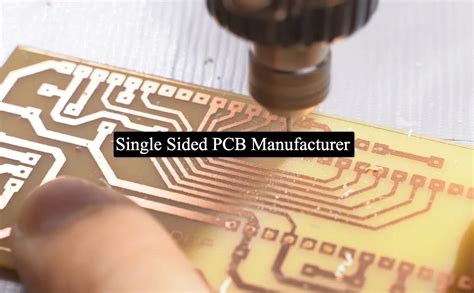
Streamlining Single-Sided Board Assembly Processes
Key Takeaways
Effective PCB assembly processes rely on optimizing both manual and automated workflows to balance speed and precision. For single-sided board assembly, prioritizing strategic soldering methods—such as selective wave soldering or reflow techniques—ensures consistent electrical connections while minimizing thermal stress. Implementing automated optical inspection (AOI) systems enhances quality control by detecting solder joint defects or misaligned components early in the PCBA cycle.
Streamlining component placement strategies—like grouping similar parts or optimizing feeder configurations—reduces machine idle time and accelerates throughput. Cost efficiency is further achieved by standardizing material selections and leveraging bulk procurement for high-use components. Transitioning to modular fixture designs also supports rapid reconfiguration for diverse board layouts.
A critical factor in PCB assembly success lies in integrating data-driven analytics to monitor production bottlenecks. Pairing real-time performance metrics with predictive maintenance schedules ensures equipment reliability, reducing unplanned downtime. When combined with staff training on lean manufacturing principles, these approaches create a cohesive workflow that aligns with modern PCBA demands for scalability and repeatability.
Optimizing Single-Sided PCB Assembly Workflows
Efficient PCB assembly processes for single-sided boards rely on harmonizing design, material selection, and automation. A streamlined workflow begins with optimizing the component placement sequence to minimize manual handling. By prioritizing high-density areas and grouping similar components, manufacturers can reduce PCBA cycle times by up to 20%. Strategic solder paste application further enhances consistency, particularly when paired with stencil designs tailored to single-sided layouts.
| Process Stage | Key Optimization | Impact |
|---|---|---|
| Design Review | Component clustering | Reduces placement errors |
| Stencil Printing | Laser-cut apertures | Improves solder deposition |
| Reflow Soldering | Profile calibration | Minimizes thermal stress |
Automated inspection protocols, such as automated optical inspection (AOI), play a critical role in identifying defects early. Integrating AOI systems post-reflow ensures alignment with IPC-A-610 standards while reducing rework costs. For PCBA workflows, balancing automation with operator oversight in low-volume batches maintains flexibility without compromising speed. Transitioning to modular assembly lines also allows rapid adaptation to design changes, ensuring scalability for both prototype and production runs. By aligning these strategies, manufacturers achieve repeatable quality while meeting tight tolerances inherent in single-sided board applications.
Cost-Effective Techniques for Board Assembly
Implementing cost-effective strategies in PCB assembly requires balancing efficiency with quality. A critical starting point is optimizing material selection—choosing standardized components and cost-efficient substrates without compromising performance. For instance, using PCBA-compatible solder alloys with lower melting points can reduce energy consumption during reflow processes while maintaining joint integrity.
"Prioritize component placement symmetry to minimize soldering defects and rework. A well-planned layout reduces thermal stress and improves PCB assembly consistency."
Automated pick-and-place systems enhance accuracy and speed, particularly for high-volume PCBA production. Pairing this with wave soldering for through-hole components ensures uniform solder distribution, reducing material waste. Additionally, adopting modular tooling designs allows quick changeovers between batches, cutting downtime by up to 30%.
Cost savings also emerge from rigorous process validation. Pre-production simulations identify potential bottlenecks, while statistical process control (SPC) monitors yield rates in real time. For example, integrating automated optical inspection (AOI) systems early in the PCB assembly line catches defects before downstream stages, avoiding costly reflows.
Finally, collaborating with suppliers to standardize component footprints and packaging formats streamlines inventory management. This reduces procurement lead times and minimizes excess stock—key factors in sustaining lean PCBA operations. By aligning these techniques, manufacturers achieve scalable cost reductions without sacrificing reliability.
Strategic Soldering Methods for Enhanced Quality
Effective soldering remains the cornerstone of reliable PCB assembly, particularly for single-sided boards where precision directly impacts performance. Implementing wave soldering for high-volume production ensures consistent solder joint formation, while selective soldering targets specific components, minimizing thermal stress on sensitive parts. For PCBA workflows, optimizing solder paste application through stencil design reduces bridging risks, especially with fine-pitch components.
Temperature profiling is critical—maintaining peak reflow temperatures within ±5°C of specifications prevents cold joints or component degradation. Pairing this with nitrogen-assisted soldering environments minimizes oxidation, enhancing electrical conductivity. Post-soldering, automated optical inspection (AOI) systems validate joint integrity, flagging defects like insufficient wetting or tombstoning early in the PCB assembly process.
Transitioning from manual to robotic soldering systems further elevates repeatability, particularly in PCBA lines handling mixed-technology boards. By integrating real-time monitoring tools, manufacturers can dynamically adjust parameters, aligning with lean production principles. These strategies not only bolster quality but also create a seamless handoff to subsequent stages, such as automated inspection, ensuring cohesive workflow progression.
Automated Inspection in PCB Assembly Quality
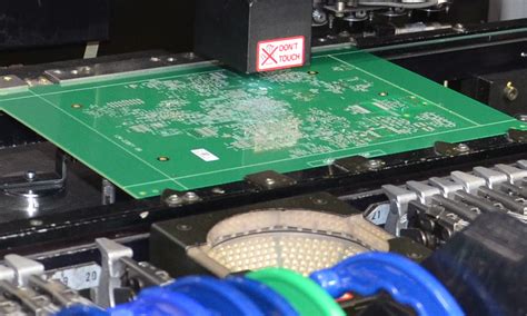
Automated inspection has become a critical component in modern PCB assembly workflows, ensuring consistent quality while addressing the precision demands of PCBA manufacturing. Advanced automated optical inspection (AOI) systems now leverage high-resolution cameras and machine learning algorithms to detect micro-level defects, such as solder bridging, component misalignment, or insufficient solder joints, with accuracy rates exceeding 99.5%. These systems integrate seamlessly with pick-and-place machines and reflow ovens, creating a closed-loop feedback mechanism that adjusts process parameters in real time.
In PCBA production, automated inspection reduces human error by 60–80% compared to manual checks, directly lowering rework costs and cycle times. For single-sided boards, where component density is typically lower, AOI focuses on verifying polarity alignment and solder fillet integrity, critical for boards with through-hole components. Furthermore, automated X-ray inspection (AXI) complements AOI by examining hidden connections, such as those beneath surface-mounted devices, ensuring no voids or cracks compromise electrical reliability.
By implementing statistical process control (SPC) protocols, manufacturers correlate inspection data with production variables, enabling predictive maintenance and process optimization. This data-driven approach not only elevates quality standards but also aligns with cost-reduction goals outlined in broader PCB assembly strategies. As automation evolves, its role in maintaining traceability and compliance across high-volume production runs becomes indispensable for competitive manufacturing ecosystems.
Streamlining Component Placement Strategies
Effective PCB assembly relies on precision in component placement, particularly for single-sided boards where spatial constraints demand meticulous planning. Optimizing this stage begins with design-for-manufacturing (DFM) principles, which prioritize logical component grouping based on function, thermal requirements, and signal pathways. For instance, placing heat-sensitive parts away from high-power components minimizes thermal interference, while aligning connectors along board edges simplifies post-assembly integration.
Modern PCBA workflows increasingly leverage automated pick-and-place systems to enhance accuracy and throughput. These systems utilize vision-guided robotics to position components within ±0.05mm tolerances, reducing human error and rework rates. However, even with automation, strategic planning remains critical. Engineers must balance placement density against accessibility for soldering and inspection—overcrowding can lead to shadowing effects during reflow, compromising joint quality.
Transitioning seamlessly from design to production requires close collaboration between layout engineers and assembly teams. Standardizing footprint libraries and orientation guidelines ensures consistency across batches, while real-time feedback loops from inspection systems allow rapid adjustments. By refining these strategies, manufacturers can achieve faster cycle times, lower material waste, and improved yield rates in PCB assembly processes.
Reducing Production Costs in Board Assembly
Cost reduction in PCB assembly requires a holistic approach that balances efficiency with quality. One primary strategy involves optimizing material utilization by leveraging precise panelization techniques for single-sided boards, minimizing substrate waste. Implementing design-for-manufacturing (DFM) principles early in the design phase ensures components are positioned to reduce soldering complexity and material overlap, directly lowering PCBA expenses.
Another key driver is automated component placement, which accelerates throughput while reducing human error. Pairing this with standardized solder paste application methods—such as stencil printing—ensures consistent PCB assembly quality, avoiding rework costs. For high-volume orders, bulk purchasing of common components like resistors and capacitors further trims expenses through economies of scale.
Additionally, integrating predictive maintenance for assembly equipment minimizes downtime, preserving production schedules. Advanced PCBA workflows also benefit from real-time monitoring systems that identify inefficiencies in energy use or material flow. By adopting modular tooling setups, manufacturers can swiftly adapt to design changes without costly retooling delays.
Finally, partnering with suppliers for just-in-time inventory management reduces storage overhead while ensuring component availability. These strategies, when combined, create a leaner PCB assembly process that aligns cost efficiency with the reliability demanded by modern electronics manufacturing.
Efficient Single-Sided Board Assembly Solutions
Achieving efficiency in PCB assembly for single-sided boards hinges on balancing precision with scalability. A central focus lies in optimizing component placement strategies, where careful planning minimizes trace lengths and reduces signal interference. Leveraging PCBA automation tools, such as pick-and-place systems, accelerates throughput while maintaining alignment accuracy—critical for high-volume production. For cost-sensitive projects, integrating surface-mount devices (SMDs) alongside through-hole components can maximize board space utilization without compromising reliability.
Strategic soldering techniques further enhance workflow efficiency. Wave soldering remains a staple for single-sided boards, but selective soldering systems now offer targeted heat application, reducing thermal stress on sensitive components. Pairing these methods with automated optical inspection (AOI) ensures consistent joint quality, catching defects like cold solder or misalignments early in the process. Manufacturers adopting PCB assembly best practices often report 15-20% faster cycle times compared to manual workflows.
To maintain competitiveness, aligning PCBA processes with design-for-manufacturing (DFM) principles is essential. This includes standardizing component libraries and adhering to panelization guidelines to minimize material waste. As equipment advancements continue to refine automated inspection protocols, the integration of real-time analytics further streamlines decision-making, bridging the gap between production speed and end-product quality.
Workflow Enhancements for PCB Manufacturing
Modern PCB assembly processes demand systematic improvements to address the unique challenges of single-sided board production. By integrating automated pick-and-place systems, manufacturers can achieve precision in component placement, reducing human error and cycle times. Advanced solder paste application techniques, such as laser-guided stenciling, ensure consistent deposition, which is critical for high-yield soldering on single-sided PCBA. Pairing these methods with optimized reflow profiles minimizes thermal stress, enhancing joint reliability while maintaining throughput.
Transitioning to modular workflow designs allows for seamless integration of automated optical inspection (AOI) systems. These tools detect soldering defects or misaligned components in real time, preventing costly rework downstream. For cost-sensitive projects, adopting predictive maintenance algorithms on assembly equipment reduces unplanned downtime, aligning with broader goals of reducing production costs. Additionally, digitizing workflow documentation ensures traceability across PCB assembly stages, enabling rapid troubleshooting.
By balancing automation with lean manufacturing principles, manufacturers can streamline PCBA workflows without compromising flexibility. This approach not only accelerates time-to-market but also creates a scalable framework adaptable to evolving single-sided board design requirements.
Conclusion
In the evolving landscape of electronics manufacturing, refining single-sided board assembly workflows remains pivotal for balancing efficiency and precision. By integrating strategic soldering techniques and optimizing component placement protocols, manufacturers can significantly reduce production costs while maintaining stringent quality benchmarks. The adoption of automated inspection systems in PCB assembly not only minimizes human error but also accelerates defect detection, ensuring consistent output across high-volume orders.
For PCBA specialists, prioritizing workflow standardization—from solder paste application to final testing—creates a repeatable framework that mitigates bottlenecks. Emphasizing data-driven adjustments to machine calibration and material selection further enhances throughput without compromising reliability. As industries increasingly demand cost-effective yet robust solutions, leveraging these advancements in single-sided board assembly will remain critical for staying competitive. Ultimately, the synergy between optimized processes and advanced automation defines the future of efficient PCB manufacturing.
FAQs
What are the key benefits of optimizing single-sided board assembly workflows?
Optimizing workflows in PCB assembly reduces manual errors and accelerates production cycles. By implementing strategic soldering techniques and automated inspection, manufacturers achieve consistent quality while lowering PCBA costs.
How do automated inspection protocols enhance assembly quality?
Automated systems detect soldering defects, misaligned components, and trace inconsistencies with higher precision than manual checks. This ensures compliance with PCB assembly standards and minimizes post-production rework.
Can component placement strategies impact production costs?
Yes. Streamlining placement through panelization and standardized layouts reduces material waste and machine idle time. For PCBA projects, this translates to faster turnaround and improved resource utilization.
What soldering methods are most effective for single-sided boards?
Wave soldering remains a cost-efficient choice for high-volume runs, while selective soldering suits mixed-technology boards. Both methods, when calibrated for thermal profiles, prevent pad lifting and ensure reliable joints in PCB assembly.
How can manufacturers balance quality and cost in single-sided board assembly?
Adopting modular tooling, predictive maintenance, and real-time monitoring systems optimizes both parameters. For tailored PCBA solutions, partner with experts who specialize in scalable workflows.
Ready to Optimize Your PCB Assembly Process?
For advanced PCB assembly services tailored to single-sided boards, please click here to explore custom solutions that align with your production goals.