Miniaturized PCBs: Revolutionizing Modern Electronics
Introduction
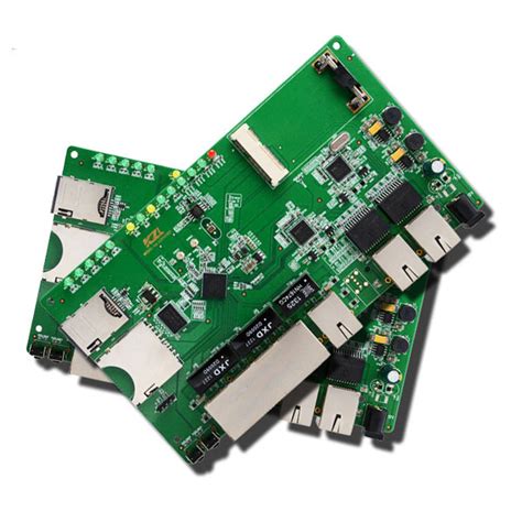
Printed Circuit Boards (PCBs) are the backbone of modern electronics, providing the foundation for interconnecting electronic components. As technology advances, the demand for smaller, lighter, and more efficient electronic devices has led to the development of miniaturized PCBs. These compact PCBs enable the creation of portable, high-performance devices used in consumer electronics, medical equipment, aerospace, and IoT applications.
This article explores the design challenges, manufacturing techniques, materials, and applications of miniaturized PCBs, highlighting their role in shaping the future of electronics.
1. What Are Miniaturized PCBs?
Miniaturized PCBs are smaller, high-density circuit boards designed to fit into compact electronic devices while maintaining or improving performance. They incorporate advanced design techniques such as:
- High-Density Interconnect (HDI) technology – Allows for finer traces, smaller vias, and tighter component placement.
- Embedded components – Resistors, capacitors, and even ICs are embedded within the PCB layers to save space.
- Flex and rigid-flex PCBs – Combine flexibility with miniaturization for wearable and foldable electronics.
These advancements enable devices like smartphones, smartwatches, medical implants, and drones to become smaller without sacrificing functionality.
2. Design Challenges in Miniaturized PCBs
Designing miniaturized PCBs presents several challenges:
A. Signal Integrity and Crosstalk
- As traces become thinner and closer together, electromagnetic interference (EMI) and crosstalk increase.
- Solution: Careful impedance control, shielding, and differential signaling techniques.
B. Thermal Management
- Smaller boards have less surface area for heat dissipation, leading to potential overheating.
- Solution: Use of thermal vias, heat sinks, and advanced substrate materials like metal-core PCBs.
C. Manufacturing Tolerances
- Ultra-fine traces (as small as 25µm) require high-precision fabrication.
- Solution: Laser drilling and direct imaging (DI) for precise etching.
D. Component Placement
- Miniaturization demands smaller components (0201, 01005 packages) and advanced assembly techniques.
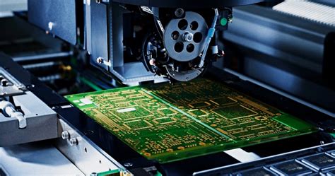
- Solution: Automated pick-and-place machines and reflow soldering with tight process control.
3. Manufacturing Techniques for Miniaturized PCBs
A. High-Density Interconnect (HDI) Technology
- Uses microvias (laser-drilled holes <100µm) to connect multiple layers.
- Enables stacked and staggered vias for complex routing.
B. Sequential Lamination
- Multiple thin layers are laminated sequentially to achieve high-density routing.
- Used in smartphone motherboards and RF modules.
C. Embedded Component Technology
- Passive (resistors, capacitors) and active (ICs) components are embedded inside the PCB.
- Reduces surface footprint and improves electrical performance.
D. Advanced Substrate Materials
- Low-loss dielectrics (Rogers, Teflon) for high-frequency applications.
- Flexible substrates (polyimide) for bendable electronics.
4. Applications of Miniaturized PCBs
A. Consumer Electronics
- Smartphones & Wearables: Apple Watch, AirPods, and foldable phones rely on HDI PCBs.
- IoT Devices: Sensors and smart home devices use compact PCBs for wireless connectivity.
B. Medical Devices
- Implantable Electronics: Pacemakers and neurostimulators require ultra-small, biocompatible PCBs.
- Portable Diagnostics: Glucose monitors and wearable health trackers use flexible PCBs.
C. Aerospace & Defense
- Drones & Satellites: Weight reduction is critical; mini PCBs enable compact avionics.
- Military Comms: Ruggedized HDI PCBs for secure, high-speed data transmission.
D. Automotive Electronics
- ADAS (Advanced Driver Assistance Systems): Miniaturized PCBs power LiDAR and radar sensors.
- Electric Vehicles (EVs): Battery management systems (BMS) use high-density PCBs.
5. Future Trends in Miniaturized PCBs
A. 3D-Printed Electronics
- Additive manufacturing allows custom-shaped PCBs with embedded components.
B. AI-Optimized PCB Design
- Machine learning algorithms optimize routing for signal integrity and thermal performance.
C. Ultra-Thin & Transparent PCBs
- Emerging for flexible displays and augmented reality (AR) glasses.
D. Quantum Computing Interconnects
- Miniaturized superconducting PCBs for quantum processors.
Conclusion
Miniaturized PCBs are transforming the electronics industry, enabling smaller, faster, and more efficient devices. Despite challenges in signal integrity, thermal management, and manufacturing precision, advancements in HDI technology, embedded components, and flexible substrates continue to push the boundaries of what’s possible.
As 5G, IoT, AI, and quantum computing evolve, the demand for ultra-compact PCBs will only grow. Engineers and manufacturers must continue innovating to meet these demands, ensuring that miniaturized PCBs remain at the heart of next-generation electronics.