PCB Cloning: Techniques, Applications, and Ethical Considerations
1. Introduction
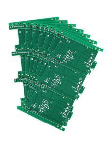
Printed Circuit Board (PCB) cloning is the process of replicating an existing PCB design to create an identical or functionally equivalent board. This practice is widely used in electronics manufacturing, reverse engineering, and product maintenance. While PCB cloning offers significant benefits in terms of cost savings and rapid prototyping, it also raises ethical and legal concerns, particularly regarding intellectual property (IP) rights.
This article explores the techniques involved in PCB cloning, its applications, the tools used, and the ethical considerations surrounding this practice.
2. PCB Cloning Techniques
The process of PCB cloning involves several steps, from analyzing the original board to producing a functional replica. Below are the key techniques used:
2.1 Physical Inspection and Imaging
The first step in PCB cloning is a thorough physical inspection of the original board. High-resolution imaging techniques, such as:
- Microscopic imaging (for fine-pitch components)
- X-ray imaging (for multi-layer PCBs)
- 3D scanning (for complex layouts)
These methods help in capturing the exact placement of components, traces, and vias.
2.2 Schematic Reverse Engineering
After obtaining images of the PCB, the next step is to reverse-engineer the schematic diagram. This involves:
- Identifying components (resistors, capacitors, ICs, etc.)
- Tracing connections between components
- Reconstructing the circuit logic
Software tools like Altium Designer, KiCad, or Eagle are often used to redraw the schematic.
2.3 PCB Layout Recreation
Once the schematic is ready, the PCB layout must be recreated. This includes:
- Layer-by-layer analysis (for multi-layer PCBs)
- Trace width and spacing replication
- Pad and via placement
Advanced PCB design software can automate parts of this process by importing scanned images and converting them into editable layouts.
2.4 Testing and Validation
After cloning, the new PCB must be tested to ensure functionality matches the original. Common validation methods include:
- Continuity testing (checking for open/short circuits)
- Signal integrity analysis (for high-speed designs)
- Functional testing (verifying performance under real conditions)

3. Applications of PCB Cloning
PCB cloning serves various purposes across industries, including:
3.1 Legacy System Maintenance
Many industries rely on outdated electronics that are no longer in production. PCB cloning allows manufacturers to:
- Repair obsolete equipment (medical devices, military hardware)
- Replace discontinued PCBs without redesigning from scratch
3.2 Competitive Analysis and Reverse Engineering
Companies may clone PCBs to:
- Analyze competitors’ designs
- Improve upon existing products
- Develop compatible components
3.3 Rapid Prototyping and Cost Reduction
Instead of designing a new PCB, cloning can:
- Accelerate development cycles
- Reduce R&D costs
- Enable small-scale production
3.4 Counterfeit Electronics and Unauthorized Replication
Unfortunately, PCB cloning is also used unethically to:
- Produce counterfeit electronics
- Bypass licensing agreements
- Infringe on patented designs
4. Tools and Software for PCB Cloning
Several tools facilitate the PCB cloning process:
4.1 Hardware Tools
- Multimeters & Oscilloscopes (for signal analysis)
- PCB Scanners (high-resolution imaging)
- Desoldering Stations (component removal for analysis)
4.2 Software Tools
- PCB Design Software (Altium, KiCad, Cadence)
- Image-to-Schematic Converters (ScanCAD, PCB Router)
- Signal Simulation Tools (LTspice, PSpice)
4.3 Automated PCB Cloning Machines
Some advanced systems can:
- Scan and replicate PCBs automatically
- Generate Gerber files directly from physical boards

5. Ethical and Legal Considerations
While PCB cloning has legitimate uses, it also poses ethical and legal challenges:
5.1 Intellectual Property (IP) Violations
- Patents – Copying a patented PCB design without permission is illegal.
- Copyrights – Schematics and layouts may be protected under copyright law.
- Trade Secrets – Cloning proprietary designs may lead to legal action.
5.2 Counterfeit Electronics
Cloned PCBs are sometimes sold as genuine products, leading to:
- Safety risks (faulty medical/military equipment)
- Economic losses for original manufacturers
5.3 Best Practices for Ethical Cloning
To avoid legal issues, companies should:
- Obtain permission from the original designer
- Use cloning only for repair/maintenance
- Avoid selling cloned PCBs as original products
6. Conclusion
PCB cloning is a powerful technique with applications in electronics repair, reverse engineering, and competitive analysis. However, it must be used responsibly to avoid IP violations and counterfeit production.
As technology advances, PCB cloning tools will become more sophisticated, making it easier to replicate complex designs. The industry must balance innovation with ethical practices to ensure fair competition and protect intellectual property.
By understanding the techniques, applications, and legal implications of PCB cloning, engineers and manufacturers can leverage its benefits while avoiding potential pitfalls.
