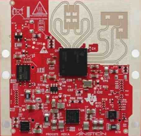
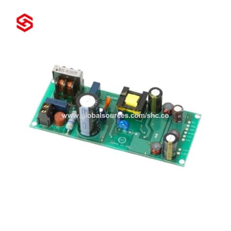
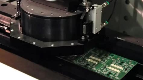
Rapid PCB Assembly: High-Speed Solutions for Time-Sensitive Projects

Key Takeaways
Modern PCB assembly processes leverage high-speed automation and optimized workflows to meet urgent project deadlines without compromising quality. By integrating advanced surface-mount technology (SMT) and automated pick-and-place systems, manufacturers achieve faster PCBA cycles while maintaining precision. Critical to success is the alignment of design-for-manufacturability (DFM) checks with rapid prototyping, ensuring minimal rework and faster validation.
For time-sensitive projects, just-in-time material sourcing reduces idle periods, and real-time collaboration between design and production teams accelerates problem resolution. Additionally, automated optical inspection (AOI) and X-ray verification systems guarantee reliability even under compressed timelines. These strategies collectively enable 24-hour turnaround options for prototypes and small batches, catering to industries like IoT, automotive, and medical devices where speed-to-market is critical.
By prioritizing streamlined workflows and cutting-edge equipment, rapid PCB assembly services deliver cost-effective scalability for urgent electronics development, balancing speed with the rigorous standards required for functional, durable boards.

High-Speed PCB Assembly Techniques
Modern PCB assembly relies on advanced methodologies to meet the demands of time-sensitive projects. By integrating automated pick-and-place systems and laser-aligned soldering, manufacturers achieve component placement accuracy within microns, reducing errors that could delay production. For PCBA workflows, high-speed surface-mount technology (SMT) enables the placement of up to 30,000 components per hour, while in-line optical inspection (AOI) ensures quality without compromising speed.
Tip: Optimize designs for manufacturability (DFM) by collaborating with assembly partners early. This minimizes revisions and accelerates turnaround.
A critical factor in rapid PCB assembly is the synchronization of fabrication and assembly stages. For example:
| Technique | Traditional Timeline | High-Speed Timeline |
|---|---|---|
| Component Placement | 8–12 hours | 2–4 hours |
| Soldering & Reflow | 6–8 hours | 1–3 hours |
| Quality Assurance | 24–48 hours | 4–8 hours |
Furthermore, just-in-time material sourcing and pre-validated component libraries eliminate bottlenecks. Advanced PCBA providers also employ predictive thermal modeling to prevent soldering defects, ensuring reliability even under accelerated timelines. By balancing speed with precision, these techniques enable electronics developers to meet aggressive project milestones without sacrificing performance.

Fast-Track PCB Production Methods
To meet urgent project deadlines, manufacturers employ fast-track PCB production methods that optimize every stage of PCB assembly (PCBA). By integrating automated pick-and-place systems with advanced soldering technologies, production lines achieve dramatic reductions in cycle times without compromising precision. Real-time process monitoring ensures seamless coordination between design validation, component procurement, and assembly workflows, minimizing bottlenecks.
A critical element involves leveraging high-speed surface-mount technology (SMT) to place microcomponents at rates exceeding 50,000 placements per hour. Concurrently, design-for-manufacturability (DFM) checks are performed during prototyping to preempt revisions, accelerating time-to-market. For rapid PCB assembly, suppliers often maintain inventories of common ICs and connectors, bypassing extended lead times.
Advanced optical inspection (AOI) systems further streamline quality assurance, identifying defects within minutes rather than hours. These fast-track methods are particularly vital for IoT devices and medical equipment, where time-sensitive iterations demand both speed and reliability. By balancing accelerated timelines with rigorous testing protocols, manufacturers ensure that PCBA outputs meet performance benchmarks even under compressed schedules.
Cutting-Edge PCB Assembly Technologies
Modern PCB assembly relies on advanced technologies to meet the demands of time-sensitive projects. Innovations like automated optical inspection (AOI) systems and 3D solder paste inspection (SPI) ensure precision during PCBA, minimizing defects and rework. High-speed pick-and-place machines, equipped with AI-driven vision systems, accurately position components at rates exceeding 50,000 placements per hour, significantly accelerating production cycles.
Another critical innovation is the integration of laser direct imaging (LDI), which enhances circuit pattern accuracy for complex designs, reducing alignment errors. Additionally, advanced soldering techniques such as vapor phase reflow offer uniform thermal distribution, critical for high-density interconnects in compact electronics. These technologies not only streamline PCB assembly but also maintain stringent quality standards, even under tight deadlines.
Emerging tools like in-line testing systems further optimize workflows by performing real-time electrical validation, eliminating bottlenecks in post-assembly diagnostics. Combined with cloud-based project management platforms, these solutions enable seamless coordination between design, fabrication, and testing phases. By leveraging these cutting-edge methods, manufacturers achieve faster PCBA turnaround without compromising reliability—a necessity for industries like aerospace, medical devices, and IoT development.

Time-Sensitive Electronics Manufacturing Solutions
Meeting tight deadlines in electronics development demands PCB assembly workflows optimized for speed without compromising quality. For projects requiring accelerated timelines, manufacturers leverage PCBA (printed circuit board assembly) strategies that integrate high-speed automation with rigorous quality checks. Advanced pick-and-place systems, combined with AI-driven inspection tools, enable rapid component placement while minimizing errors. To further reduce lead times, just-in-time material sourcing and pre-validated design templates ensure seamless transitions from prototyping to full-scale production.
Critical to these solutions is the synchronization of PCB fabrication and assembly stages. By employing parallel processing—where board fabrication and component procurement occur simultaneously—teams shave days off traditional schedules. Additionally, DFM (design for manufacturability) analysis is conducted upfront to eliminate redesign delays, ensuring designs are production-ready from the first iteration. For mission-critical applications, such as medical devices or aerospace systems, real-time monitoring systems track every assembly step, guaranteeing compliance with industry standards even under compressed timelines.
These methodologies not only address urgent project needs but also maintain the reliability required for complex electronics. By balancing rapid PCB assembly with precision engineering, manufacturers deliver time-sensitive solutions that align with evolving market demands.

Streamlined Processes for Quick PCB Results
Modern PCB assembly relies on optimized workflows that eliminate bottlenecks while maintaining rigorous quality standards. By integrating automated pick-and-place systems with just-in-time material sourcing, manufacturers achieve faster cycle times without compromising precision. Advanced PCBA lines now employ parallel processing, where multiple stages—such as solder paste application, component placement, and reflow soldering—operate synchronously. This method reduces idle time between production phases, particularly critical for prototypes or low-volume batches requiring rapid iteration.
Real-time monitoring tools further enhance efficiency by identifying potential delays in assembly sequences, allowing immediate adjustments. For instance, automated optical inspection (AOI) systems verify solder joint integrity during the assembly process, preventing post-production rework. Additionally, standardized design-for-manufacturing (DFM) checks ensure files are production-ready, minimizing back-and-forth revisions. When combined with pre-validated component libraries, these practices accelerate PCB assembly timelines by up to 40% compared to traditional methods.
Supply chain integration plays a pivotal role, with certified vendors providing guaranteed lead times for critical parts. This end-to-end coordination ensures that PCBA projects transition seamlessly from design to delivery, meeting even the most aggressive deadlines. By prioritizing process automation and data-driven decision-making, manufacturers deliver consistent results while adapting to evolving project requirements.

Precision in Rapid Circuit Board Assembly
While speed remains critical in PCB assembly for time-sensitive projects, maintaining precision is non-negotiable. Advanced PCBA workflows integrate automated optical inspection (AOI) systems and laser-aligned pick-and-place machines to ensure micron-level accuracy, even under accelerated timelines. These technologies minimize human error while verifying solder joint integrity, component alignment, and trace connectivity in real time.
To balance velocity with reliability, manufacturers employ predictive modeling to anticipate thermal stresses and signal interference risks during high-speed production. This proactive approach enables adjustments in PCB assembly parameters before physical fabrication begins, preserving quality without compromising deadlines. For mission-critical applications, such as medical devices or aerospace systems, cross-functional verification protocols validate electrical performance against design specifications at multiple checkpoints.
The synergy between PCBA automation and rigorous quality control ensures that rapid turnarounds do not sacrifice precision. By combining surface-mount technology (SMT) with intelligent design-for-manufacturability (DFM) checks, teams achieve first-pass success rates exceeding 98%, even for complex multilayer boards. This precision-centric strategy not only accelerates production but also reduces costly revisions, making it indispensable for electronics projects where both speed and reliability are paramount.
Reducing PCB Fabrication Timelines Effectively
Achieving shorter PCB assembly cycles requires a strategic blend of advanced engineering practices and process optimization. By leveraging design for manufacturability (DFM) principles, engineers can preemptively address potential bottlenecks, ensuring layouts align with automated PCBA workflows. Modern fabrication facilities employ high-speed pick-and-place systems and laser-direct imaging (LDI) to accelerate component placement and circuit patterning, slashing production time by up to 40%. Concurrently, just-in-time material sourcing minimizes delays, while real-time quality checks via automated optical inspection (AOI) maintain reliability without compromising speed.
For time-sensitive projects, adopting parallel processing—where multiple fabrication stages occur simultaneously—can further compress timelines. For instance, prototyping and testing phases often overlap in rapid PCB assembly workflows, enabling iterative refinements without halting production. Additionally, partnerships with certified PCBA providers offering expedited shipping and 24/7 manufacturing support ensure seamless transitions from design to delivery. By integrating these methodologies, teams can reliably meet tight deadlines while upholding the precision required for complex electronics, making rapid fabrication a sustainable advantage in competitive markets.
Rapid Prototyping for Urgent Electronics Projects
In time-sensitive electronics development, PCB assembly processes must align with accelerated prototyping cycles to meet critical deadlines. Modern rapid prototyping techniques integrate directly with PCBA workflows, enabling engineers to validate designs within hours instead of days. By leveraging 3D printing for enclosure fabrication and automated optical inspection (AOI) for instant quality checks, teams can identify design flaws before full-scale production begins. This approach reduces iterative delays while maintaining the precision required for complex circuits. Advanced surface-mount technology (SMT) lines further compress timelines by populating boards 60% faster than manual methods. For projects requiring functional validation under 72 hours, on-demand component sourcing paired with parallel testing protocols ensures all subsystems meet performance benchmarks simultaneously. These synchronized strategies allow developers to advance from concept to certified prototype without compromising on signal integrity or thermal management standards, even when working with high-density interconnects or mixed-technology boards.
Conclusion
In today’s fast-paced electronics landscape, the ability to execute rapid PCB assembly is no longer a luxury but a necessity for meeting stringent project deadlines. By integrating automated assembly lines with advanced PCBA workflows, manufacturers can drastically compress production cycles without compromising on precision. This approach ensures that time-sensitive projects—from IoT devices to medical equipment—benefit from high-yield manufacturing while adhering to rigorous quality standards.
Key to achieving these results is the strategic use of just-in-time component sourcing and PCB assembly processes optimized for speed. Techniques such as laser-direct imaging and automated optical inspection (AOI) minimize human intervention, reducing errors and accelerating validation phases. Additionally, collaborative design-for-manufacturability (DFM) reviews enable early detection of potential bottlenecks, further streamlining timelines.
Ultimately, the convergence of cutting-edge technologies and lean methodologies in PCBA services empowers engineers to deliver functional prototypes and end-use products at unprecedented speeds. As manufacturers continue to refine their rapid-turn capabilities, businesses gain a critical edge in markets where being first often defines success. The future of electronics development hinges on this balance: precision, speed, and unwavering reliability.
FAQs
How does rapid PCB assembly differ from standard production methods?
Rapid PCBA prioritizes compressed timelines through automated workflows, parallel processing, and just-in-time material sourcing. Unlike conventional approaches, it leverages real-time design validation and pre-certified components to eliminate bottlenecks.
What minimum turnaround can be achieved with expedited PCB assembly services?
Advanced providers deliver PCBA prototypes in 24-48 hours and full production batches within 5-7 days. These timelines depend on design complexity and component availability, with optimized DFM (Design for Manufacturing) checks ensuring faster approvals.
Does accelerated production compromise PCB assembly quality?
Reputable manufacturers maintain ISO-certified processes, combining automated optical inspection (AOI) and X-ray testing even in rapid workflows. Statistical process control ensures defect rates remain below 0.1%, matching standard production benchmarks.
Which industries benefit most from rapid PCB assembly solutions?
Medical devices, aerospace systems, and IoT infrastructure rely on PCBA speed for prototype iterations and field upgrades. Automotive electrification projects also use these services to meet stringent regulatory deadlines.
How can I prepare files to optimize PCB assembly speed?
Submit Gerber/ODB++ files with annotated layer stacks, component placement maps, and BOM (Bill of Materials) containing manufacturer-specific part numbers. Pre-approving panelization designs reduces back-and-forth revisions.
Accelerate Your Time-Sensitive PCB Projects
For tailored PCB assembly solutions that align with urgent deadlines, please click here to consult our engineering team. We specialize in high-mix, low-volume PCBA with guaranteed rapid turnaround.
