Precision Engineering: Flex PCB Fabrication Techniques for Optimal Reliability
Key Takeaways
When designing flexible circuits, understanding core fabrication principles directly impacts PCB manufacturing outcomes. You’ll need to balance bend radii with material properties—exceeding mechanical limits risks delamination, while overly conservative designs add unnecessary bulk. Leading PCB manufacturing companies prioritize polyimide substrates for their thermal stability, but newer liquid crystal polymer (LCP) options offer superior high-frequency performance in compact layouts.
Stiffener integration demands precision: mismatched thickness or adhesive choices create stress points during dynamic flexing. For example, stainless steel stiffeners excel in high-vibration environments but increase PCB manufacturing cost, whereas FR-4 alternatives reduce weight without sacrificing rigidity.
| Factor | Consideration | Impact on Reliability |
|---|---|---|
| Bend Radius | ≥10x material thickness | Prevents micro-cracking |
| Adhesive Type | Acrylic vs. epoxy performance | Affects thermal cycling endurance |
| Stiffener Placement | Strategic component anchoring | Reduces torsion stress |
Weight reduction strategies, such as laser-ablation thinning, require collaboration with PCB manufacturing business partners who offer advanced prototyping tools. Domestic suppliers often provide faster iteration cycles, critical for aerospace or medical applications where validation timelines compress. By aligning design intent with production capabilities early, you mitigate risks in scaling from prototype to volume runs—a hallmark of competitive PCB manufacturing ecosystems.
Flex PCB Fabrication Precision Techniques
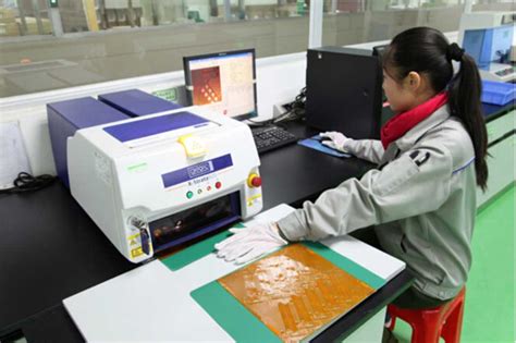
Achieving optimal reliability in flex PCB manufacturing begins with mastering precision techniques that balance performance with structural integrity. When designing flexible circuits, you must prioritize controlled etching processes to maintain consistent trace widths, ensuring signal integrity even under repeated bending. Partnering with experienced PCB manufacturing companies ensures access to laser-direct imaging (LDI) systems, which achieve micron-level accuracy for intricate layouts.
"Always validate material compatibility early in design—mismatched coefficients of thermal expansion between layers can cause delamination during dynamic operation."
To minimize PCB manufacturing cost, focus on optimizing panel utilization during fabrication. Advanced adhesives like acrylic or epoxy blends enhance layer bonding while accommodating flex cycles. For high-frequency applications, consider polyimide substrates with low dielectric loss, paired with rolled annealed copper for improved fatigue resistance.
Integrating stiffeners requires precision placement—use laser-cut stainless steel or FR-4 sections to reinforce connector areas without compromising flexibility. Modern PCB manufacturing business practices leverage automated optical inspection (https://www.andwinpcba.com) to tailor designs for extreme environments, from aerospace to wearable tech.
By aligning your design strategy with these techniques, you ensure durability without unnecessary weight—a critical balance for applications demanding both reliability and compact form factors. Next, we’ll examine how bend radius optimization further safeguards against mechanical failure.
Optimizing Bend Radius for Reliability
When designing flexible circuits, managing bend radius becomes critical to maintaining long-term performance in dynamic applications. You’ll want to calculate the minimum allowable curvature based on material thickness and copper type—exceeding this limit risks microfractures that compromise electrical integrity. For single-layer flex PCBs, a general rule is to keep bends at least 6x the substrate thickness, while multilayer designs often require 10–12x to account for stacked materials.
Leading PCB manufacturing companies leverage simulation tools to model stress distribution during repeated flexing, ensuring designs align with mechanical fatigue thresholds. This precision reduces PCB manufacturing cost by minimizing field failures and warranty claims. If you’re balancing weight reduction with reliability, consider tapered stiffeners or selective reinforcement at high-stress points—techniques refined by advanced PCB manufacturing business workflows.
Transitioning from prototype to production? Validate bend cycles under real-world conditions early. Partnering with PCB manufacturing experts ensures compliance with IPC-2223 standards, which define testing protocols for flex circuit durability. Remember: tighter bends may save space, but they’ll elevate long-term risks. Prioritize controlled curvature to harmonize flexibility with operational lifespan.
Advanced Material Selection Strategies
When designing flexible circuits, your choice of materials directly impacts durability, thermal stability, and PCB manufacturing cost. Leading PCB manufacturing companies prioritize polyimide films for their unmatched flex endurance and resistance to extreme temperatures (-269°C to 400°C). For high-frequency applications, liquid crystal polymer (LCP) substrates reduce signal loss while maintaining mechanical resilience—critical for aerospace or medical devices.
Adhesive systems matter just as much. Acrylic-based options offer rapid bonding for quick-turn prototypes, whereas epoxy adhesives provide stronger bonds for industrial-grade assemblies. To optimize PCB manufacturing business workflows, consider hybrid material stacks that balance performance and affordability. For instance, pairing thin stainless-steel stiffeners with polyimide layers enhances structural integrity without compromising flexibility.
Conductive materials also require scrutiny. Rolled annealed copper improves cyclic bending performance compared to electrodeposited alternatives, while silver-based inks enable stretchable traces for wearable tech. Always validate material compatibility with your PCB manufacturing partner to avoid delamination or impedance mismatches during dynamic operation.
By aligning material properties with application demands—whether prioritizing weight reduction or extreme-environment reliability—you ensure designs meet both technical and budgetary targets without over-engineering.
Stiffener Integration in Flexible Circuits
When designing flexible circuits for PCB manufacturing, strategic stiffener integration becomes critical to balancing flexibility and structural support. Stiffeners—typically made from materials like FR4, polyimide, or aluminum—are laminated to specific circuit areas to prevent mechanical stress in dynamic applications. For instance, connectors or component-heavy zones require rigid reinforcements to maintain Z-axis stability during repeated bending.
PCB manufacturing companies often recommend matching stiffener thickness to your application’s bend radius requirements. A 0.1mm polyimide stiffener might suffice for wearable electronics, while industrial sensors could demand thicker FR4 layers. However, over-engineering stiffeners risks increasing PCB manufacturing cost and negating weight-saving advantages. Advanced adhesives and laser-cut profiles now enable precise alignment, ensuring stiffeners enhance durability without compromising the circuit’s inherent pliability.
For PCB manufacturing business models targeting high-reliability sectors—aerospace, medical devices, or automotive—stiffener integration must account for thermal expansion coefficients and environmental stressors. Partnering with manufacturers experienced in multi-material hybrid designs ensures optimal performance. Remember: stiffeners aren’t just add-ons—they’re precision-engineered solutions to extend product lifetimes in demanding conditions.

Dynamic Application Durability Solutions
When designing flexible circuits for high-stress environments, achieving lasting durability requires balancing mechanical resilience with functional performance. You’ll need to prioritize materials and configurations that withstand repeated bending, vibration, and temperature fluctuations. Leading PCB manufacturing companies recommend using polyimide substrates paired with rolled annealed copper, as these combinations maintain conductivity while resisting fatigue cracks.
For dynamic applications like robotics or wearable tech, optimizing bend radius becomes critical—exceeding material limits risks delamination or trace fractures. Advanced simulation tools help validate designs before production, reducing PCB manufacturing cost by minimizing trial-and-error iterations. Reinforcing high-stress areas with laser-cut stiffeners or strategic adhesive placement ensures localized rigidity without compromising overall flexibility.
Environmental factors also play a role. Partnering with PCB manufacturing businesses that offer conformal coatings or encapsulation services adds moisture and chemical resistance, extending product lifespans in harsh conditions. Testing protocols, including cyclic flexing and thermal shock simulations, verify performance thresholds before scaling to volume production. By aligning material science with application-specific stressors, you create solutions that endure real-world demands while maintaining cost efficiency.
Weight Reduction in PCB Architecture
Achieving weight reduction in flexible circuit designs requires strategic engineering decisions that align with modern miniaturization trends and performance demands. By opting for ultra-thin polyimide films (as low as 12.5 μm) and selective copper etching, you reduce material bulk without compromising conductivity. Advanced pcb manufacturing companies leverage high-density interconnect (HDI) techniques to eliminate unnecessary connectors, further trimming mass in multi-layer configurations.
When evaluating pcb manufacturing cost, consider trade-offs between material choices and long-term reliability. For instance, adhesiveless laminates cut 20-30% of substrate weight compared to traditional bonded materials, but their integration demands precision tooling. Partnering with pcb manufacturing experts ensures optimal stiffener placement—using localized polyamide or FR4 reinforcements—to balance structural integrity and weight savings.
In high-mobility applications like aerospace or wearables, every gram matters. Here, pcb manufacturing business models prioritizing iterative prototyping allow you to validate designs for dynamic stress resistance before full-scale production. Techniques such as laser-cut geometries and 3D modeling software refine component layouts, reducing redundant traces and enclosures. This holistic approach not only meets weight targets but also aligns with broader goals of durability and pcb manufacturing efficiency.
Prototype-to-Production Support Systems
When transitioning from design validation to full-scale manufacturing, PCB manufacturing companies provide critical infrastructure to bridge the gap between concept and reality. These systems integrate design-for-manufacturability (DFM) analysis tools, automated workflow tracking, and multi-stage testing protocols to ensure seamless scalability. By collaborating closely with engineering teams, manufacturers identify potential bottlenecks early—whether in PCB manufacturing cost drivers like material waste or in tolerance mismatches during high-frequency signal routing.
Modern support frameworks leverage iterative prototyping to refine flex PCB designs, using advanced simulations to predict mechanical stress points and thermal performance under dynamic conditions. This phase often includes real-world bend testing to validate reliability before committing to production volumes. For businesses managing PCB manufacturing business operations, such systems reduce time-to-market by 30–50% through standardized documentation templates and cloud-based project dashboards that centralize communication.
Key to this process is balancing customization with cost efficiency. Reputable partners offer tiered service models, allowing you to scale from low-volume prototypes to mass production without redesigning tooling or sacrificing quality controls. Look for providers that combine ISO 9001-certified processes with transparent PCB manufacturing cost breakdowns, ensuring you maintain budget predictability while achieving MIL-spec durability in critical applications.
USA-Based Flex PCB Manufacturing Benefits
When sourcing PCB manufacturing partners, choosing domestic providers offers distinct advantages for high-reliability flexible circuits. Proximity to PCB manufacturing companies in the U.S. reduces lead times by minimizing logistical delays, enabling faster design iterations and tighter collaboration during prototyping. This geographic advantage also simplifies compliance with industry-specific standards like ITAR or MIL-PRF-31032, critical for aerospace or defense applications where traceability and material certifications are non-negotiable.
Domestic PCB manufacturing cost structures often align better with low-to-mid-volume production runs, particularly when balancing advanced material requirements (e.g., polyimide films) against tighter tolerance controls. Local suppliers typically provide transparent pricing models without hidden tariffs or import fees, allowing you to optimize budgets while maintaining quality. Additionally, U.S.-based PCB manufacturing business ecosystems prioritize intellectual property protection, ensuring proprietary flex designs remain secure throughout the production lifecycle.
By partnering with American manufacturers, you gain access to vertically integrated facilities that combine material science expertise with precision fabrication tools—key for achieving consistent bend cycles and thermal stability in dynamic environments. This localized approach not only strengthens supply chain resilience but also supports sustainability goals through reduced carbon footprints and adherence to stricter environmental regulations.
Conclusion
When navigating the complexities of PCB manufacturing, your choices in PCB manufacturing companies directly influence both performance and PCB manufacturing cost. Selecting partners with expertise in dynamic environments ensures designs meet rigorous reliability standards while balancing economic viability. By prioritizing precision in bend radius optimization and material compatibility, you mitigate risks of failure in applications requiring repeated flexing.
Integrating stiffeners and lightweight architectures requires collaboration with PCB manufacturing business specialists who understand how structural enhancements impact thermal management and mechanical stress. This partnership becomes critical when transitioning from prototype to full-scale production, where even minor design flaws can escalate costs.
For projects demanding tight tolerances, domestic PCB manufacturing offers advantages like streamlined communication and adherence to stringent quality controls. While offshore options might reduce upfront expenses, local expertise often delivers better long-term value by minimizing rework and accelerating time-to-market. Ultimately, aligning your fabrication strategy with application-specific requirements ensures durable, high-performance flexible circuits without compromising on weight or functionality.
Frequently Asked Questions
How does material selection impact flex PCB reliability?
Choosing the right dielectric materials and copper alloys ensures resistance to thermal stress and mechanical fatigue. Partnering with experienced PCB manufacturing companies helps balance performance with PCB manufacturing cost, especially for high-frequency or extreme-environment applications.
What role do stiffeners play in flexible circuits?
Stiffeners enhance structural stability in areas requiring component mounting or connector insertion. Proper integration prevents flexural failures while maintaining weight reduction goals—a critical consideration for aerospace or wearable tech PCB manufacturing business models.
Why is bend radius optimization crucial for dynamic applications?
Exceeding the minimum bend radius risks conductor cracking. Advanced PCB manufacturing processes use simulation tools to validate bend cycles, ensuring durability in folding displays or robotic assemblies.
How do US-based manufacturers ensure quality control?
Domestic PCB manufacturing companies adhere to IPC-6013 standards, combining automated inspection with rigorous testing. This reduces defect rates by up to 40% compared to offshore alternatives, aligning with strict industry certifications.
Can prototyping reduce long-term production costs?
Yes. Iterative prototyping identifies design flaws early, minimizing material waste. Many PCB manufacturing providers offer scalable solutions—from 10-unit batches to mass production—optimizing PCB manufacturing cost across product lifecycles.
Ready to Optimize Your Flex PCB Project?
For tailored support in PCB manufacturing—from prototype validation to full-scale production—please click here: https://www.andwinpcb.com/pcb-manufacturing/.