Where Does PCB Come From? Understanding the Origins and Production of Printed Circuit Boards
Introduction to PCB Origins
Printed Circuit Boards (PCBs) form the foundational infrastructure of modern electronics, serving as the physical platform that connects and supports electronic components in everything from smartphones to spacecraft. But where does this essential technology come from? The origins of PCBs trace back over a century, with their production evolving through numerous technological revolutions to become the sophisticated manufacturing process we know today.
The story of PCBs begins in the early 20th century, but their widespread adoption didn’t occur until after World War II. Today, the global PCB market exceeds $80 billion annually, reflecting their critical role in our increasingly digital world. Understanding where PCBs come from involves exploring both their historical development and their modern manufacturing processes across global supply chains.
This article will examine the historical development of PCB technology, the raw materials used in their production, the detailed manufacturing process, the global supply chain that delivers them, and emerging innovations that are shaping their future.
Historical Development of PCB Technology
The concept behind printed circuit boards emerged in the early 20th century when inventors began exploring ways to simplify the complex wiring in electronic devices. German inventor Albert Hanson is often credited with the earliest patent resembling a PCB in 1903, describing a flat foil conductor laminated to an insulating board with multiple layers.
In the 1920s, American inventor Charles Ducas developed a method for creating an electrical path directly on an insulated surface by printing through a stencil with electrically conductive inks—the first true “printed” wiring. However, these early innovations saw limited commercial application until the pressures of World War II drove technological advancement.
The modern PCB as we know it was developed by Austrian engineer Paul Eisler while working in England during the 1940s. Eisler’s innovation involved etching conductive copper foil bonded to a non-conductive substrate, creating precise circuit pathways. This method was first used extensively in proximity fuses for artillery shells, proving its reliability in demanding conditions.
Post-war commercialization saw PCBs gradually replace point-to-point wiring in consumer electronics throughout the 1950s and 1960s. The U.S. Army’s development of the Auto-Sembly process in the 1950s automated PCB component insertion, while the introduction of integrated circuits in the 1960s increased PCB complexity and miniaturization.
Key milestones in PCB evolution include:
- 1936: First use of PCBs in radios
- 1948: U.S. commercial PCB production begins
- 1950s: Introduction of double-sided boards
- 1960s: Development of multilayer boards
- 1980s: Surface-mount technology revolution
- 2000s: High-density interconnect (HDI) microvias
Raw Materials: The Building Blocks of PCBs
Understanding where PCBs come from begins with their fundamental materials. A typical PCB consists of several essential components, each sourced from different materials with specific properties.
The substrate, or base material, is usually a glass-reinforced epoxy laminate known as FR-4 (Flame Retardant 4). This composite material combines woven fiberglass cloth with an epoxy resin binder, offering excellent mechanical strength, electrical insulation, and flame resistance. The fiberglass comes from silica sand melted and drawn into fine fibers, while the epoxy resin derives from petroleum products through chemical synthesis.
The conductive pathways are made from copper foil, which constitutes the second primary material in PCBs. Copper is chosen for its exceptional electrical conductivity and relatively low cost. PCB manufacturers typically use electrodeposited or rolled copper foil ranging from 1/4 oz to 2 oz per square foot in thickness (about 8.5 μm to 70 μm). Major copper producers include Chile, Peru, China, and the United States.
Additional materials include:
- Solder mask: A polymer layer (usually green) that insulates copper traces
- Silkscreen: Epoxy ink for component labels and identifiers
- Metallic finishes: Such as gold, silver, or tin for surface protection
- Adhesives: For multilayer board construction
- Via fill materials: For creating conductive connections between layers
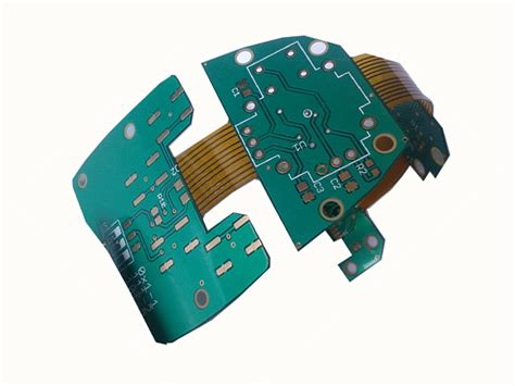
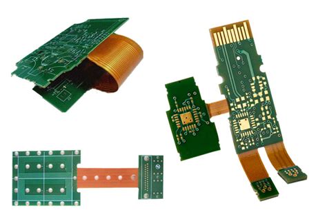
The selection of materials depends on the PCB’s intended application. High-frequency applications might use PTFE (Teflon) substrates, while flexible electronics use polyimide films. Environmental concerns have driven development of halogen-free and biodegradable materials in recent years.
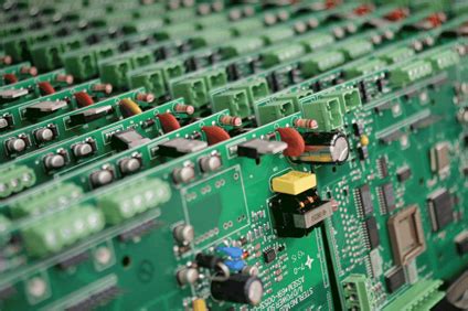
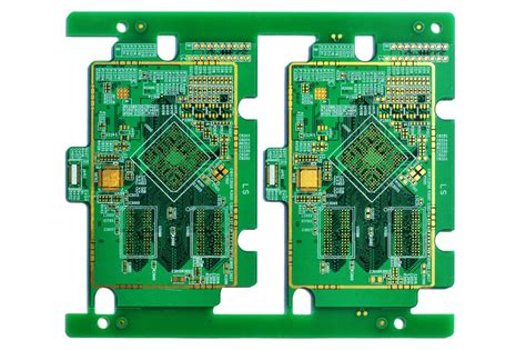
The PCB Manufacturing Process: From Design to Finished Product
PCB production is a complex, multi-stage process that transforms raw materials into functional circuit boards. Modern PCB manufacturing typically involves the following key steps:
- Design and Preproduction:
- Circuit design using ECAD software
- Design rule checking (DRC) to ensure manufacturability
- Gerber file generation for manufacturing instructions
- Substrate Preparation:
- Cutting laminate material to size
- Cleaning surfaces for proper adhesion
- Patterning (Image Transfer):
- Applying photoresist to copper-clad laminate
- Exposing to UV light through photomask
- Developing to remove unexposed resist (for negative resist)
- Etching:
- Chemical removal of unwanted copper (typically with ammonium persulfate or ferric chloride)
- Stripping remaining photoresist
- Layer Alignment and Lamination (for multilayer boards):
- Prepeg (pre-impregnated) dielectric layers sandwiched between copper layers
- Heat and pressure application to cure resin
- Drilling:
- Mechanical or laser drilling of holes for vias and component leads
- Desmearing to remove drilling debris
- Plating and Coating:
- Electroless copper deposition to make hole walls conductive
- Electroplating to build up copper thickness
- Application of surface finishes (HASL, ENIG, OSP)
- Solder Mask Application:
- Liquid photoimageable (LPI) solder mask coating
- UV exposure and development to expose pads
- Silkscreen Printing:
- Component identifiers and logos
- Curing of epoxy ink
- Testing and Quality Control:
- Automated optical inspection (AOI)
- Electrical testing (flying probe or bed-of-nails)
- Final verification against specifications
Advanced PCB types like HDI (High Density Interconnect) or flexible circuits involve additional specialized processes such as laser drilling of microvias or precision flex-circuit handling systems.
Global PCB Production and Supply Chain
The production of PCBs has become a truly global enterprise, with manufacturing concentrated in Asia but serving markets worldwide. Understanding where PCBs come from geographically reveals much about modern electronics manufacturing.
China dominates global PCB production, accounting for over 50% of worldwide output. Major Chinese PCB manufacturing clusters exist in:
- Guangdong province (Shenzhen, Guangzhou, Dongguan)
- Jiangsu province (Suzhou, Kunshan)
- Shanghai municipality
Other significant Asian producers include:
- Taiwan: Known for high-end and advanced PCB technologies
- South Korea: Specializing in high-density interconnect boards
- Japan: Focused on high-reliability and specialty PCBs
- Southeast Asia: Growing production in Vietnam, Thailand, and Malaysia
Outside Asia, notable PCB manufacturing exists in:
- United States: Primarily high-reliability/military applications
- Germany: Precision and automotive electronics
- Israel: Advanced technologies and R&D
The PCB supply chain involves multiple tiers:
- Raw material suppliers (copper, fiberglass, chemicals)
- Laminate manufacturers (producing copper-clad substrates)
- PCB fabricators (producing bare boards)
- Electronics manufacturing services (assembling components)
- Original equipment manufacturers (final products)
Recent trends have seen some reshoring of PCB production due to:
- Supply chain disruptions (e.g., COVID-19 pandemic)
- Geopolitical tensions and trade wars
- Demand for shorter lead times
- Quality control requirements in critical industries
Future Trends and Environmental Considerations
As electronics continue to evolve, so too does PCB technology. Several key trends are shaping where future PCBs will come from both technologically and geographically:
Technological Advancements:
- Higher density interconnects with smaller features
- Embedded components within the PCB structure
- 3D printed electronics and additive manufacturing
- Integration of passive components into the substrate
- Advanced materials for high-frequency 5G and mmWave applications
Environmental and Sustainability Developments:
- Lead-free and halogen-free materials
- Improved recycling processes for end-of-life PCBs
- Biodegradable substrate materials research
- Reduced water and chemical usage in manufacturing
- Renewable energy use in production facilities
Geopolitical and Economic Shifts:
- Regionalization of supply chains for resilience
- Increased automation in high-cost regions
- Growth of PCB recycling infrastructure
- Stricter regulations on hazardous substances (RoHS, REACH)
The drive toward sustainability is particularly significant, as traditional PCB manufacturing involves numerous toxic chemicals and generates hazardous waste. New approaches include:
- Chemical recycling of copper and precious metals
- Recovery and reuse of etching solutions
- Dry processes that eliminate wastewater
- Plant-based epoxy resins and natural fiber reinforcements
As these trends develop, the answer to “where do PCBs come from” may involve more localized production, greener materials, and advanced manufacturing methods that reduce environmental impact while meeting the growing demands of our digital world.
Conclusion: The Continuing Evolution of PCB Origins
From their early 20th century beginnings to today’s sophisticated global manufacturing network, printed circuit boards have undergone remarkable transformation. What began as simple conductive patterns on Bakelite has evolved into multilayer, high-density interconnects with microscopic features produced through highly automated processes.
The question “where does PCB come from” encompasses both geographical origins and technological genesis. Physically, most PCBs originate from Asian factories with specialized equipment and expertise. Technologically, they emerge from a century of accumulated knowledge in materials science, chemical engineering, and precision manufacturing.
Looking ahead, PCB production continues to evolve in response to technological demands and environmental imperatives. The next generation of PCBs may come from entirely different materials and processes—perhaps 3D printed with conductive polymers or grown from biologically derived substrates. What remains constant is the essential role these unassuming boards play in enabling all modern electronics, connecting our world one circuit at a time.
Understanding PCB origins gives us appreciation for this foundational technology and insight into the future directions of electronics manufacturing. As devices become smarter, smaller, and more ubiquitous, the humble PCB will continue its quiet revolution beneath the surface of our digital lives.