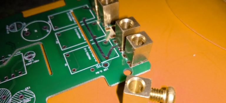
Gerber File Essentials for PCB Design Success

Key Takeaways
When preparing files for PCB manufacturing, understanding Gerber format essentials ensures your design translates accurately into physical boards. Start by recognizing that PCB manufacturing companies rely on these files to etch copper layers, drill holes, and apply solder masks—any error here can delay production or increase PCB manufacturing cost.
Three critical steps stand out:
- Verify layer alignment: Misaligned copper and solder mask layers cause short circuits.
- Include all required files: Aperture lists, drill files, and board outlines are non-negotiable.
- Optimize for compatibility: While Gerber (RS-274X) remains the universal standard, formats like ODB++ or IPC-2581 offer richer data for complex designs.
Tip: Always run a *Design for Manufacturing (https://www.andwinpcba.com) help spot inconsistencies early.
If you’re scaling a PCB manufacturing business, balancing precision with efficiency is key. For example, consolidating layers in Gerber reduces parsing errors, while standardized naming conventions streamline communication with fabricators. Remember, even minor oversights—like missing drill tables—can derail timelines and inflate budgets. By mastering these fundamentals, you ensure seamless transitions from design to production, whether prototyping or managing high-volume orders.
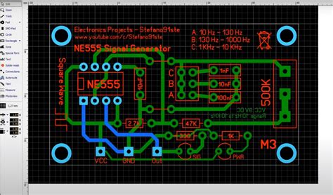
Gerber File Fundamentals Explained
Understanding Gerber files is critical when preparing designs for PCB manufacturing. These files act as a universal language between your design software and PCB manufacturing companies, translating complex layouts into precise instructions for fabrication. Each Gerber file represents a specific layer of your board—copper traces, solder mask, silkscreen—using apertures (shape definitions) and coordinates to map every detail.
When generating these files, you’ll define parameters like layer stack-up and drill locations, which directly influence PCB manufacturing cost and timeline. For example, incorrect aperture sizing or misaligned layers can lead to production delays, forcing manufacturers to request revisions. This is why standardized formats like RS-274X (Extended Gerber) are preferred—they embed critical data, reducing ambiguity.
While alternatives like ODB++ or IPC-2581 exist, Gerber remains the default for most PCB manufacturing business operations. To ensure compatibility, verify that your design tool exports files in the correct format and resolution. Always cross-check layer assignments and aperture lists before submission—small oversights here can escalate into costly errors during fabrication. By mastering these fundamentals, you streamline communication with manufacturers and minimize risks in the production pipeline.

PCB Format Comparison: Gerber Alternatives
While Gerber files remain the industry standard for PCB manufacturing, modern alternatives like ODB++ and IPC-2581 offer enhanced capabilities for complex designs. Understanding these formats ensures compatibility with PCB manufacturing companies and optimizes PCB manufacturing cost by reducing rework.
| Format | Data Structure | Layer Handling | Adoption in PCB Manufacturing Business |
|---|---|---|---|
| Gerber RS-274X | 2D image-based | Single-layer files | Universal (90%+ factories) |
| ODB++ | Intelligent hierarchy | Multi-layer bundles | Growing (40% of advanced facilities) |
| IPC-2581 | Parametric data | Unified XML schema | Emerging (adopted by major OEMs) |
ODB++ consolidates design data into a single archive, reducing file count and minimizing human error during transfers—a critical advantage for PCB manufacturing workflows. Its structured format improves communication between designers and fabricators, streamlining design-for-manufacturing (DFM) checks. Meanwhile, IPC-2581 integrates material specs and tolerances directly into the file, enabling automated validation that lowers PCB manufacturing cost by catching errors early.
When selecting a format, consider your PCB manufacturing companies’ capabilities. While Gerber ensures broad compatibility, ODB++ and IPC-2581 enhance precision for high-density or high-frequency boards. Balancing standardization with advanced features ensures your PCB manufacturing business avoids delays and maintains cost-efficiency across projects.
From Design to Production: Gerber Process
The journey from circuit design to functional hardware hinges on how effectively you translate your schematic into PCB manufacturing specifications. This is where Gerber files act as the universal language, bridging the gap between design software and fabrication equipment. When preparing these files, you’ll define copper layers, solder masks, silkscreens, and drill data—each layer meticulously mapped to guide PCB manufacturing companies in replicating your board precisely.
To minimize PCB manufacturing cost, ensure your Gerber files adhere to your fabricator’s design rules. Even minor oversights—like missing aperture definitions or misaligned layers—can trigger delays or rework. Modern tools let you export RS-274X (Extended Gerber) or ODB++ formats, which embed metadata to reduce interpretation errors. For complex designs, some PCB manufacturing businesses prefer IPC-2581, a standardized format that bundles all fabrication data into a single file, streamlining communication.
Before finalizing, run automated checks to verify layer consistency and drill overlaps. Collaborating early with your manufacturer ensures alignment on file formats and tolerances, preventing costly revisions. By mastering this process, you transform abstract designs into manufacturable blueprints—a critical step in scaling prototypes to production-ready solutions.
Ensuring PCB Accuracy via Gerber Files
Precision in PCB manufacturing begins with correctly formatted Gerber files, which act as the universal language between your design software and fabrication equipment. To avoid costly revisions, verify that every layer—copper traces, solder mask, silkscreen, and drill data—aligns perfectly with your board’s specifications. PCB manufacturing companies rely on these files to interpret critical details like trace widths, pad sizes, and annular ring clearances. A single mismatch in layer alignment or missing aperture definitions can trigger production errors, increasing PCB manufacturing cost and delaying timelines.
Use design rule checks (DRC) and Gerber viewers to cross-validate files before submission. Pay special attention to drill files (Excellon format) for hole placement accuracy, as even minor offsets can compromise component mounting. For multilayer boards, ensure layer stacking order and material specifications are explicitly documented in your notes. While formats like ODB++ and IPC-2581 offer enhanced data encapsulation, Gerber remains the industry standard—making its proper use non-negotiable for maintaining trust in the PCB manufacturing business.
Collaborate early with your fabrication partner to confirm their specific requirements, such as file naming conventions or copper weight notations. This proactive approach minimizes ambiguities, ensuring your design translates seamlessly into a functional, reliable circuit board.
Common Gerber File Mistakes to Avoid
Even minor errors in your Gerber files can derail PCB manufacturing timelines and inflate PCB manufacturing costs. One frequent oversight is neglecting to include all necessary layers—missing solder mask or silkscreen layers often force PCB manufacturing companies to halt production for clarification. Another critical error involves improper file naming conventions. Ambiguous labels like "Layer1.gbr" create confusion, especially when working with global partners in the PCB manufacturing business. Always use standardized names (e.g., "TopCopper.gbr" or "BottomMask.gbr") to eliminate ambiguity.
Failing to verify design rule checks (DRC) before exporting files is equally risky. Overlooked clearance violations or unconnected traces may pass schematic checks but render boards unmanufacturable. Additionally, using outdated Gerber formats like RS-274X without confirming compatibility with your manufacturer’s equipment can lead to parsing errors. Modern alternatives like ODB++ or IPC-2581 offer richer data, but inconsistent format adoption between designers and PCB manufacturing teams remains a pain point.
Finally, skipping a thorough visual review using a Gerber viewer often results in undetected flaws like misaligned drills or flipped layers. These mistakes compound PCB manufacturing costs through rework fees and delayed deliveries. Always cross-reference your files with your manufacturer’s specifications to ensure seamless handoff.
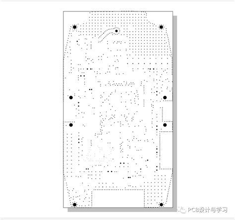
Gerber File Generation Step-by-Step
To create Gerber files for PCB manufacturing, begin by finalizing your board design in CAD software. Verify layer alignment and design rules to prevent errors that could increase PCB manufacturing cost. Most tools offer export wizards—navigate to the Gerber generation section and select layers (copper, solder mask, silkscreen) individually.
Next, configure drill files (Excellon format) alongside Gerber outputs. These specify hole locations and sizes, critical for PCB manufacturing companies to fabricate boards accurately. Double-check file extensions: .GTL (top layer), .GBL (bottom layer), and .DRL (drill file) are standard.
After exporting, use a Gerber viewer to simulate how manufacturers will interpret your data. Look for mismatched apertures or missing layers—common oversights that delay production. Some designers share previews with PCB manufacturing business partners early to validate compatibility with their equipment.
Finally, compress all files into a single .ZIP folder, naming conventions clearly (e.g., ProjectName_Rev1_Gerber). Include a readme.txt file listing layers and special instructions. This structured approach minimizes revisions, ensuring your design transitions smoothly from concept to fabrication.
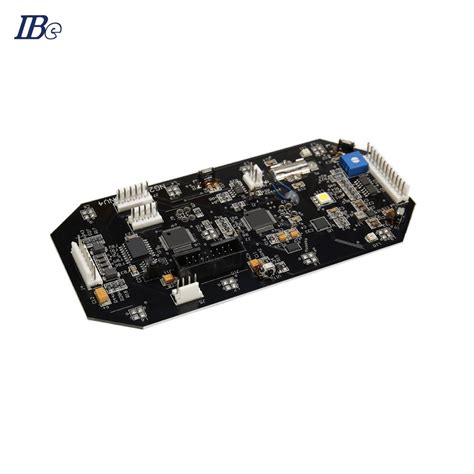
Optimizing Gerber Files for Manufacturing
When preparing Gerber files for PCB manufacturing, precision is non-negotiable. Start by verifying your design against your manufacturer’s guidelines—common oversights like missing solder mask layers or unclear drill files can delay production and inflate PCB manufacturing costs. Use design rule checks (DRC) to flag potential issues early, ensuring alignment with your chosen PCB manufacturing companies’ capabilities.
Layer organization matters: label each Gerber layer descriptively (e.g., Top Copper, Soldermask_Bottom) to avoid misinterpretation. Include a detailed drill file with tool sizes and plating specifications, as ambiguities here often lead to costly rework. For complex designs, consider supplementing Gerber with ODB++ or IPC-2581 formats, which embed stack-up details and material specifications directly, streamlining communication with your PCB manufacturing business partner.
Optimize apertures by merging duplicate shapes and eliminating unused symbols—this reduces file size and processing time. Finally, cross-validate your output with a Gerber viewer to confirm layer alignment and critical clearances. By refining these elements, you ensure manufacturability while maintaining tight control over timelines and budgets.
Advanced Gerber Techniques Explained
To elevate your PCB manufacturing outcomes, mastering advanced Gerber file techniques is critical. Start by defining layer stack-up specifications in your Gerber files, ensuring PCB manufacturing companies receive explicit material thickness and dielectric constants. This eliminates guesswork during fabrication, directly impacting PCB manufacturing cost by reducing material waste and rework.
Implement controlled impedance routing annotations for high-speed designs. By embedding impedance values and trace geometry in Gerber layers, you enable precise signal integrity adjustments before production. Pair this with step-and-repeat patterns for panelized designs—a technique that optimizes board space utilization, lowering per-unit expenses for your PCB manufacturing business.
Leverage embedded component markers to flag parts requiring special handling, such as RF shields or thermal pads. Use aperture macros for complex copper shapes, ensuring consistency across drill hits and solder mask layers. These practices minimize discrepancies that could delay approvals with PCB manufacturing partners.
Finally, validate files using 3D Gerber viewers to simulate physical board assembly. This step catches interlayer misalignments early, preventing costly revisions. By integrating these methods, you align design intent with manufacturing realities, streamlining workflows while maintaining tight control over PCB manufacturing cost and timelines.
Conclusion
When preparing your design for PCB manufacturing, understanding how Gerber files function within the production workflow is critical. These files act as the universal language between your design software and PCB manufacturing companies, ensuring your board’s specifications are interpreted accurately. By mastering Gerber file generation, you directly influence PCB manufacturing cost efficiency—errors in layer alignment or missing drill data can lead to costly revisions or delayed timelines.
To maintain competitiveness in the PCB manufacturing business, prioritize consistency in file formats (Gerber, ODB++, or IPC-2581) and validate outputs through automated verification tools. This minimizes misinterpretation risks and aligns your deliverables with industry standards. Remember, even minor oversights—like incorrect aperture definitions—can cascade into production bottlenecks.
Ultimately, your ability to optimize Gerber files determines not just board quality but also your partnership with manufacturers. By adhering to design-for-manufacturing principles and staying updated on evolving standards, you ensure seamless transitions from prototype to mass production. Whether you’re a startup or an established enterprise, precision in this final design phase lays the groundwork for reliable, scalable outcomes.
Frequently Asked Questions
How do Gerber files impact pcb manufacturing timelines?
Properly formatted Gerber files accelerate production by providing pcb manufacturing companies with unambiguous design data. Errors in these files often lead to delays, requiring multiple revisions and increasing pcb manufacturing cost.
What file formats do manufacturers prefer besides Gerber?
While Gerber remains standard, many pcb manufacturing businesses now accept ODB++ or IPC-2581 for richer data context. Always confirm format requirements with your manufacturer to avoid compatibility issues.
Can incorrect Gerber files affect board functionality?
Yes. Missing layers or misaligned drill files can render boards unusable. Double-check copper layers, solder masks, and silkscreen details to ensure alignment with pcb manufacturing specifications.
How do you optimize files for cost-effective production?
Simplify designs where possible, adhere to design-for-manufacturing (DFM) rules, and validate files using CAM software. This reduces pcb manufacturing cost by minimizing material waste and rework.
Why do some manufacturers reject Gerber files?
Common reasons include incomplete layer sets, undefined board outlines, or mismatched apertures. Partnering with experienced pcb manufacturing companies ensures smoother file validation and faster turnaround.
Ready to Streamline Your PCB Production?
For expert guidance on optimizing Gerber files and reducing pcb manufacturing cost, please click here to connect with industry-leading professionals.

