Custom PCB Assembly for Rapid Prototyping
Key Takeaways
PCB assembly and PCBA (Printed Circuit Board Assembly) services play a pivotal role in accelerating rapid prototyping by delivering precision-engineered boards tailored to specific project requirements. Engineers leverage flexible designs to iterate quickly, reducing development cycles while maintaining rigorous quality standards. Advanced PCB assembly techniques enable fast-turnaround production, ensuring prototypes are ready for testing within days rather than weeks.
A critical advantage lies in the integration of customizable layouts and component configurations, which streamline R&D processes. For instance, PCBA providers often employ automated workflows to minimize errors and enhance consistency, directly supporting innovation in sectors like IoT, robotics, and medical devices.
| Factor | Traditional Approach | Custom PCB Assembly |
|---|---|---|
| Turnaround Time | 4-6 weeks | 1-2 weeks |
| Design Flexibility | Limited modifications | High adaptability |
| Cost Efficiency | Higher per-unit costs | Scalable pricing models |
By prioritizing high-quality materials and advanced soldering techniques, PCB assembly services ensure reliability even in complex prototypes. This approach not only accelerates time-to-market but also mitigates risks associated with design flaws, enabling engineers to focus on functional optimization and performance testing. The synergy between rapid prototyping and PCBA underscores its value in transforming conceptual designs into tangible, market-ready solutions.
Custom PCB Assembly Accelerates Prototyping
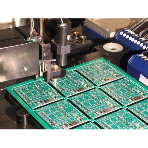
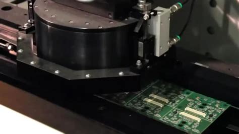
Modern PCB assembly services are redefining how engineers approach rapid prototyping, compressing timelines that once spanned weeks into days. By integrating PCBA (printed circuit board assembly) expertise with advanced manufacturing technologies, teams can iterate designs faster while maintaining rigorous quality standards. Automated pick-and-place systems, combined with precision solder paste application, ensure consistent results even for complex, multi-layer boards.
Tip: For optimal prototyping speed, prioritize PCB assembly partners offering design-for-manufacturing (DFM) feedback. Early collaboration reduces revision cycles by identifying potential issues in component placement or thermal management.
The agility of custom PCBA solutions lies in their ability to accommodate last-minute design tweaks without derailing production schedules. Modular workflows allow engineers to test multiple configurations simultaneously, accelerating validation phases. Real-time progress tracking further enhances transparency, enabling teams to align prototyping milestones with broader project timelines.
"Flexibility in component sourcing is critical—partner with PCB assembly providers maintaining diversified supplier networks to mitigate supply chain risks."
By leveraging PCBA expertise, innovators transform theoretical concepts into functional prototypes 30–50% faster than traditional methods. This acceleration is particularly impactful in industries like IoT and medical devices, where time-to-market directly correlates with competitive advantage. The result? Engineers spend less time troubleshooting manufacturing bottlenecks and more time refining breakthrough technologies.
Precision Engineering for Rapid PCB Solutions
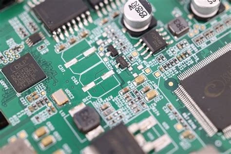
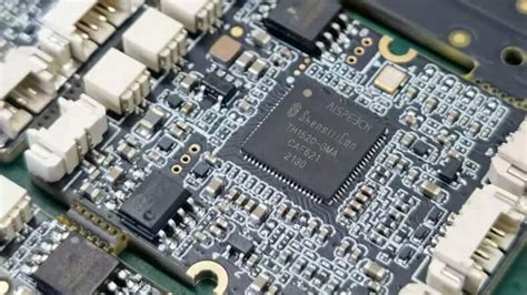
At the heart of accelerating prototyping timelines lies precision engineering in PCB assembly, which ensures that complex designs translate seamlessly into functional prototypes. Modern PCBA processes leverage advanced techniques such as surface-mount technology (SMT) and laser-drilled microvias to achieve tolerances as tight as ±0.05mm. These capabilities enable engineers to integrate high-density components, including fine-pitch BGAs and 0201 metric packages, without compromising signal integrity or thermal performance.
Critical to this precision is the use of automated optical inspection (AOI) and X-ray verification, which systematically identify soldering defects or misalignments during PCB assembly. By combining these tools with design-for-manufacturability (DFM) principles, PCBA providers reduce iterative delays, allowing teams to validate designs within days rather than weeks. This synergy between engineering rigor and flexible manufacturing workflows ensures prototypes meet exact specifications while maintaining compatibility with scalable production methods.
For innovators pushing the boundaries of IoT or embedded systems, such precision is not optional—it’s foundational. Tightly controlled PCB assembly processes eliminate guesswork, enabling rapid iteration cycles where even millimeter-level adjustments can be tested, refined, and redeployed efficiently. The result? Prototypes that mirror final-product performance, accelerating the transition from concept to market-ready solutions.
Flexible PCB Designs Streamline Development
Modern PCB assembly processes thrive on adaptability, and flexible PCB designs are proving instrumental in accelerating development cycles. By integrating PCBA solutions with bendable substrates and modular layouts, engineers gain unprecedented freedom to iterate on complex geometries without compromising functionality. This design flexibility reduces the need for multiple rigid boards, enabling compact configurations that align with evolving project requirements. For instance, dynamic routing allows signal paths to adapt to spatial constraints, while multi-layer stacking optimizes component density—critical for applications like wearables or IoT devices.
The synergy between custom PCB assembly and flexible architectures shortens validation phases, as prototypes can be tested in near-final form factors. Advanced PCBA providers now leverage software-driven simulations to predict mechanical stress points, ensuring reliability even in unconventional layouts. This approach not only minimizes physical redesigns but also enhances thermal management and signal integrity—factors that traditionally extended development timelines. By prioritizing adaptable designs early in the prototyping phase, teams can pivot faster, scale smarter, and deliver innovations that meet both technical and market demands seamlessly.
Fast-Turnaround Assembly for Prototype Innovation
In the race to bring ideas to life, PCB assembly services with accelerated timelines have become indispensable for innovators. Modern rapid prototyping relies on PCBA workflows that compress traditional production schedules by 30–60%, enabling functional testing of complex designs within days rather than weeks. This agility stems from three core elements: automated pick-and-place systems for component mounting, just-in-time material sourcing networks, and cloud-based collaboration tools that synchronize design revisions across engineering teams.
By integrating custom PCB assembly with advanced manufacturing protocols, developers gain the flexibility to test multiple iterations without derailing project timelines. For instance, high-density interconnect (HDI) boards requiring microvias or embedded components can now move from CAD files to assembled prototypes in under 72 hours. Such speed is further enhanced by design-for-manufacturability (DFM) checks embedded in the PCBA process, which preemptively resolve layout conflicts that could delay builds.
The strategic advantage lies in balancing velocity with precision—PCB assembly partners equipped with AI-driven inspection systems ensure even the fastest-turnaround prototypes meet IPC-A-610 standards. This synergy between speed and quality allows R&D teams to validate concepts faster, iterate with confidence, and ultimately compress time-to-market cycles by up to 40%.
Optimizing Development Cycles with Custom PCBs
By integrating PCB assembly services into product development workflows, engineers gain precise control over prototyping timelines. Precision-engineered boards eliminate design redundancies, while modular PCBA configurations enable swift adjustments to circuit layouts during testing phases. This approach reduces iterative delays by aligning component placement, layer stacking, and signal routing with application-specific requirements.
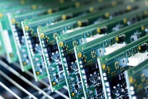
Advanced custom PCB assembly providers accelerate cycles through concurrent engineering processes, where design validation and manufacturing preparations occur in parallel. Real-time collaboration between development teams and PCBA specialists ensures immediate feedback on thermal management or impedance matching challenges. Industry data indicates projects leveraging tailored assembly solutions achieve 40–60% faster iteration speeds compared to standardized boards.
Furthermore, optimized material selection and automated PCB assembly workflows minimize post-production revisions. Rapid-turn fabrication paired with in-house component sourcing cuts lead times, allowing functional prototypes to enter verification stages within days. For R&D teams, this translates to earlier identification of design flaws and more efficient resource allocation. By adopting custom PCBs with embedded DFM (Design for Manufacturing) checks, organizations systematically compress development phases without compromising reliability—a critical advantage in industries where time-to-market dictates competitive success.
High-Quality PCB Assembly for Faster R&D
Modern research and development cycles demand PCB assembly services that prioritize both precision and speed. By leveraging advanced PCBA workflows, engineers gain access to error-free manufacturing processes that eliminate costly rework delays. High-quality assembly begins with stringent material selection, where certified components and substrates ensure reliability under rigorous testing conditions. Automated pick-and-place systems, combined with precision soldering techniques, produce boards with micron-level accuracy—critical for prototypes requiring seamless integration with complex circuitry.
A key advantage of partnering with specialized custom PCB assembly providers lies in their ability to streamline validation phases. By incorporating design-for-manufacturability (DFM) feedback early in the process, teams can identify potential bottlenecks, such as trace spacing or thermal management issues, before prototyping begins. This proactive approach reduces iterative testing, accelerating time-to-market by up to 40% in some cases. Additionally, just-in-time inventory management ensures components arrive synchronized with production schedules, avoiding downtime.
For R&D teams focused on cutting-edge applications—from IoT devices to aerospace systems—high-quality PCBA acts as a catalyst. Robust assembly standards (e.g., IPC-A-610 Class 3 compliance) guarantee durability in extreme environments, while flexible scaling options allow rapid transition from prototype validation to pilot runs. By merging technical excellence with agile workflows, custom assembly services empower innovators to compress development timelines without compromising performance benchmarks.
Custom Boards for Engineering Breakthroughs
Modern engineering challenges demand solutions that push the boundaries of conventional design, and custom PCB assembly plays a pivotal role in enabling these advancements. By leveraging PCBA (printed circuit board assembly) techniques tailored to specific project requirements, engineers can integrate specialized components, high-density interconnect (HDI) layouts, and advanced materials into compact, high-performance systems. This capability is critical for applications such as IoT devices, medical instrumentation, and aerospace systems, where miniaturization and reliability are non-negotiable.
The flexibility of custom PCB assembly allows for iterative testing of novel architectures, ensuring that prototypes align with rigorous performance benchmarks. For instance, multi-layer rigid-flex boards or embedded sensor arrays can be rapidly refined through iterative PCBA processes, reducing time-to-market for groundbreaking technologies. Additionally, partnerships with experienced assembly providers ensure access to automated optical inspection (AOI) and precision soldering, which mitigate risks during high-stakes prototyping phases.
By aligning PCB assembly strategies with cutting-edge engineering goals, teams unlock opportunities to solve previously intractable technical problems. Whether optimizing power distribution in electric vehicles or enhancing signal processing in AI-driven hardware, custom boards serve as the foundation for innovations that redefine industry standards.
Rapid Prototyping via Advanced PCB Techniques
Modern PCB assembly processes leverage cutting-edge technologies to dramatically shorten prototyping timelines. By integrating automated optical inspection (AOI) and 3D solder paste inspection (SPI), PCBA providers ensure precision while maintaining speed—critical for iterative design phases. Advanced techniques like laser direct imaging (LDI) enable finer trace resolutions, allowing engineers to test complex circuitry in early-stage prototypes without compromising functionality.
The use of surface-mount technology (SMT) paired with flexible substrate materials supports rapid design adjustments, reducing rework cycles by up to 40%. For high-frequency applications, embedded component packaging minimizes signal loss, accelerating validation of RF and IoT prototypes. These innovations in custom PCB assembly enable teams to validate designs in days rather than weeks, aligning with agile development frameworks.
Moreover, cloud-based collaboration tools now sync real-time feedback between designers and PCBA manufacturers, ensuring design-for-manufacturability (DFM) principles are applied from the first iteration. This seamless integration of engineering and production workflows eliminates bottlenecks, making advanced prototyping accessible even for low-volume, high-complexity projects.
Conclusion
The integration of custom PCB assembly into prototyping workflows underscores its pivotal role in modern engineering. By leveraging precision-engineered boards and adaptive design methodologies, teams can significantly reduce iteration time while maintaining rigorous performance standards. PCBA services, with their emphasis on flexible component sourcing and fast-turnaround manufacturing, enable innovators to validate concepts faster than traditional methods allow. This approach not only aligns with the demands of compressed development cycles but also ensures that prototypes meet exact functional specifications before scaling.
For engineers prioritizing speed without compromising quality, custom PCB assembly offers a strategic advantage—bridging the gap between conceptual designs and market-ready solutions. Advanced PCBA techniques, such as automated testing and multi-layer board fabrication, further enhance reliability during iterative testing phases. As industries increasingly adopt agile development practices, the ability to rapidly translate ideas into functional prototypes through high-quality PCBA becomes a critical differentiator. Ultimately, this synergy between tailored assembly processes and accelerated prototyping empowers teams to navigate technical challenges efficiently, driving innovation cycles forward with measurable precision.
FAQs
How does custom PCB assembly benefit rapid prototyping?
PCB assembly services enable engineers to test functional designs quickly by producing precision-engineered boards tailored to specific requirements. This reduces iterative delays and ensures prototypes align with performance benchmarks.
What distinguishes PCBA from standard PCB fabrication?
While standard fabrication focuses on bare boards, PCBA (printed circuit board assembly) integrates components like resistors and ICs, delivering fully functional prototypes ready for testing. This end-to-end process accelerates development cycles.
Can flexible designs be accommodated in custom PCB assembly?
Yes, advanced PCB assembly providers support modular layouts and multi-layer configurations, allowing engineers to experiment with compact or high-density designs without compromising turnaround speed.
How fast can I expect prototype delivery?
Leading services offer fast-turnaround PCB assembly, with some delivering fully assembled boards in 24–72 hours. This agility is critical for innovators racing to meet tight R&D deadlines.
What quality controls ensure reliable prototypes?
Reputable providers implement automated optical inspection (AOI) and X-ray testing during PCBA to verify solder integrity and component alignment, minimizing post-assembly errors.
Are low-volume orders cost-effective for prototyping?
Modern PCB assembly solutions optimize small-batch production through automated pick-and-place systems and lean workflows, making low-volume orders economically viable for iterative testing.
Ready to Accelerate Your Prototyping Process?
For tailored PCB assembly solutions that prioritize speed and precision, please click here to explore services designed for engineering breakthroughs.