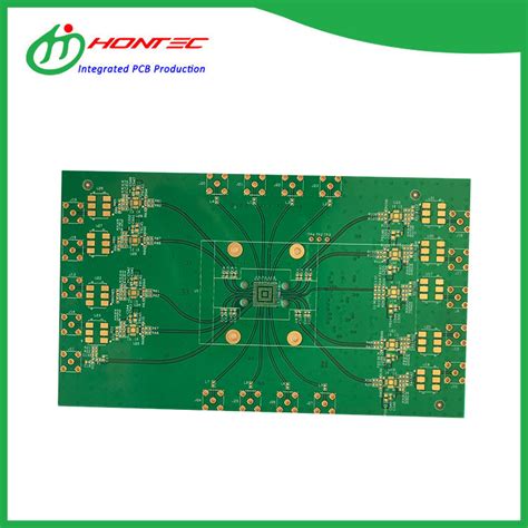
HDI Multilayer PCBs: Advancing High-Density Circuit Innovations
Key Takeaways
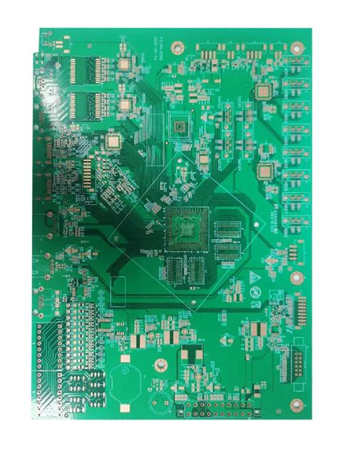
When working with HDI multilayer PCBs, understanding core design principles ensures you maximize performance while minimizing pcb manufacturing cost. These boards rely on microvia technology and precise layer stacking techniques to achieve ultra-compact layouts, enabling next-gen devices to pack more functionality into smaller footprints. For pcb manufacturing companies, balancing advanced features like laser-drilled vias with cost-efficiency remains critical, especially when scaling production for high-volume applications.
A key advantage of HDI designs lies in their ability to reduce layer counts compared to traditional PCBs, which directly impacts pcb manufacturing business workflows. For example, integrating blind and buried vias eliminates the need for through-hole drilling, saving space and materials. However, partnering with experienced manufacturers becomes essential—specialized equipment and expertise in high-density interconnect solutions ensure reliability without compromising on signal integrity.
| Factor | HDI PCB | Traditional PCB |
|---|---|---|
| Layer Count | Fewer (optimized stacking) | Higher (simple stacking) |
| Via Types | Microvias, stacked/buried | Through-hole only |
| Material Precision | High-performance substrates | Standard FR-4 |
| Manufacturing Complexity | Advanced (laser drilling) | Conventional (mechanical) |
By leveraging these innovations, you can optimize circuit density while addressing challenges like thermal management and impedance control. Whether you’re developing wearables or IoT devices, aligning your design goals with proven manufacturing strategies ensures your project stays competitive in fast-paced electronics markets.
HDI Multilayer PCB Design Principles Unveiled
When designing HDI multilayer PCBs, precision in layer arrangement and interconnect planning becomes critical. You start by prioritizing signal integrity and minimizing electromagnetic interference through optimized trace routing. Advanced PCB manufacturing companies leverage sequential lamination processes to stack multiple thin dielectric layers, enabling tighter spacing between components. This approach reduces PCB manufacturing cost by minimizing material waste while maximizing circuit density.
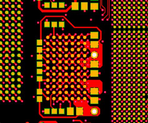
A key principle lies in using microvias and blind/buried vias to create vertical connections without occupying surface space. These microvias, often laser-drilled, allow traces to pass through inner layers, freeing up real estate for high-speed components. For PCB manufacturing businesses, balancing via density with thermal management is essential—excessive microvias can compromise structural stability if not planned with finite element analysis.
Your design must also account for impedance control, especially in high-frequency applications. By aligning dielectric constants with layer thickness, you ensure consistent signal propagation across the board. Transitioning between layers requires careful pad-to-via alignment, a task streamlined by modern EDA tools. Remember, every design choice impacts scalability; selecting materials with low thermal expansion coefficients ensures reliability during mass production.
Ultimately, HDI principles empower you to push the boundaries of miniaturization while maintaining performance—a necessity for next-gen devices demanding compact, high-speed solutions.
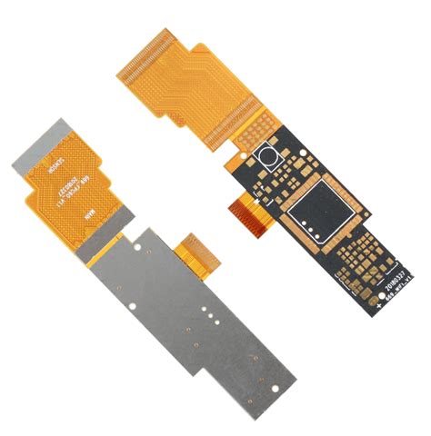
Microvia Technology in High-Density Circuit Boards
When working with HDI multilayer PCBs, you’ll find that microvia technology is central to achieving the precision required for modern electronics. Unlike traditional through-hole vias, microvias are laser-drilled interconnects smaller than 150 microns in diameter, enabling tighter circuit layouts and reducing signal loss. This innovation allows PCB manufacturing companies to pack more functionality into compact designs—critical for smartphones, wearables, and IoT devices.
Tip: To optimize PCB manufacturing cost, consider balancing microvia density with layer count early in the design phase. Overcomplicating the stack-up can increase production time and material waste.
The adoption of microvias also impacts PCB manufacturing business strategies. Advanced laser systems and specialized materials like low-loss dielectrics are essential, raising initial setup costs but offering long-term reliability benefits. For instance, staggered or stacked microvias improve thermal management in high-power applications while maintaining signal integrity.
However, not all PCB manufacturing processes are equally suited for microvia integration. You’ll need partners with expertise in sequential lamination and precise registration to avoid misalignment issues. Thermal stress during assembly remains a key challenge—choosing copper-filled microvias can enhance durability without compromising electrical performance. By prioritizing these techniques, you ensure that high-density designs meet both technical and economic demands.
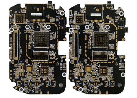
Layer Stacking Techniques for Compact PCB Manufacturing
To achieve the ultra-compact designs demanded by modern electronics, PCB manufacturing relies on advanced layer stacking methods that balance density, reliability, and thermal performance. By employing sequential lamination processes, manufacturers build high-density interconnect (HDI) boards with alternating layers of conductive and dielectric materials. This approach allows for tighter trace spacing and reduced via sizes—critical for optimizing PCB manufacturing cost while maintaining signal integrity.
Leading PCB manufacturing companies often integrate microvias and blind/buried vias within these stacked layers to minimize vertical space consumption. For instance, using laser-drilled microvias in a 10+ layer stack enables routing paths that bypass traditional through-hole vias, freeing up real estate for additional circuitry. Such techniques are particularly valuable in wearable tech or IoT devices, where board thickness directly impacts product design.
However, layer stacking introduces challenges like thermal management and interlayer alignment. To address this, manufacturers use low-CTE (coefficient of thermal expansion) materials and precision registration systems. For PCB manufacturing businesses, adopting these methods requires balancing upfront investments in equipment with long-term gains in yield and miniaturization capabilities—key differentiators in competitive markets.
By mastering these stacking strategies, you ensure your designs meet the escalating demands for high-density interconnects without compromising manufacturability or reliability.
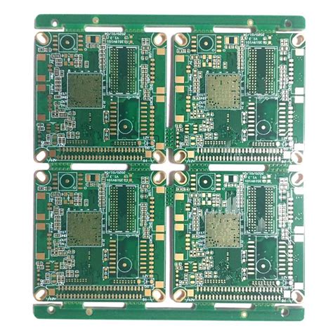
HDI vs Traditional PCBs: Key Differences Explained
When comparing HDI multilayer PCBs to traditional circuit boards, the differences lie in design complexity, material usage, and performance capabilities. While traditional PCB manufacturing relies on fewer layers and larger through-hole vias, HDI technology employs microvias, stacked layers, and finer traces to maximize space efficiency. This allows PCB manufacturing companies to achieve up to 10x higher circuit density in devices like smartphones or wearables, where miniaturization is critical.
The PCB manufacturing cost for HDI boards is initially higher due to advanced processes like laser drilling and sequential lamination. However, reduced layer counts and improved reliability often offset long-term expenses. Traditional boards, while cheaper upfront, may require more layers to match HDI’s performance, increasing material costs and design limitations.
For the PCB manufacturing business, adopting HDI means investing in specialized equipment and expertise. Unlike conventional methods, HDI demands tighter tolerances and materials like low-loss laminates to handle high-frequency signals. This shift enables ultra-compact PCB designs but also raises the bar for quality control, particularly in industries like medical tech or aerospace where precision is non-negotiable.
Ultimately, choosing between HDI and traditional PCBs hinges on balancing performance needs with PCB manufacturing realities—whether prioritizing cutting-edge density or cost-effective simplicity.
High-Density Interconnect Solutions for Modern Electronics
When designing electronics for today’s miniaturized devices, PCB manufacturing must address two critical challenges: maximizing circuit density while maintaining signal integrity. High-density interconnect (HDI) solutions achieve this by combining advanced layering techniques with precision microvia technology, enabling PCB manufacturing companies to embed more functionality into smaller footprints. Unlike conventional boards, HDI designs use stacked vias and laser-drilled holes to route traces between tightly packed components—a necessity for smartphones, wearables, and IoT devices where space is at a premium.
However, adopting HDI technology impacts PCB manufacturing cost due to the specialized equipment and materials required. For example, ultra-thin dielectric layers and copper foils demand tighter process controls, while laser drilling adds complexity. Despite this, the long-term benefits—such as reduced board size, improved thermal performance, and enhanced reliability—often justify the investment, especially for high-volume PCB manufacturing business models. By optimizing layer counts and via structures, engineers can strike a balance between performance and affordability, ensuring HDI remains accessible for both cutting-edge and cost-sensitive applications.
Transitioning to HDI requires collaboration with experienced manufacturers who understand how to navigate these trade-offs. You’ll want partners capable of scaling production without compromising on the precision that defines high-density interconnect success. This approach not only future-proofs your designs but also aligns with the evolving demands of modern electronics.
Benefits of Ultra-Compact PCB Designs in HDI
Ultra-compact HDI PCB designs unlock critical advantages for modern electronics by maximizing space efficiency without compromising performance. By integrating PCB manufacturing techniques like sequential lamination and laser-drilled microvias, these designs enable high-density interconnects that reduce overall board size by up to 70% compared to traditional layouts. This miniaturization directly benefits PCB manufacturing companies, as it allows for lighter, slimmer devices—ideal for wearables, medical implants, and aerospace systems where every millimeter matters.
The reduced footprint also lowers PCB manufacturing cost by minimizing material usage and streamlining assembly processes. Fewer layers and tighter component placement mean fewer drilling cycles and less copper waste, translating to faster production timelines. For businesses scaling their PCB manufacturing business, this efficiency creates a competitive edge, especially when paired with advanced routing algorithms that optimize signal integrity in densely packed circuits.
Additionally, ultra-compact designs enhance thermal management and electrical performance. Shorter trace lengths reduce signal loss and crosstalk, while microvias improve heat dissipation—critical for high-frequency applications. By adopting these innovations, you ensure your designs meet evolving demands for speed, reliability, and miniaturization in next-gen electronics.
Next-Gen Devices Driven by HDI PCB Innovations
At the core of this shift toward smarter, smaller electronics lies the transformative role of HDI multilayer PCBs. These boards enable devices to achieve unprecedented performance by integrating microvias and laser-drilled interconnects, which reduce signal loss while maximizing space efficiency. For PCB manufacturing companies, this means rethinking traditional processes to accommodate finer traces and tighter tolerances—a challenge that demands advanced equipment and expertise.
While some may express concerns about PCB manufacturing cost, the long-term benefits outweigh initial investments. High-density designs reduce the need for multiple boards, streamlining assembly and cutting material waste. This evolution directly impacts the PCB manufacturing business, as clients increasingly prioritize compact, high-reliability solutions for wearables, IoT sensors, and 5G infrastructure.
Leading PCB manufacturing innovators now leverage sequential lamination and embedded components to meet demands for miniaturization. These techniques not only enhance circuit density but also improve thermal management—a critical factor for devices operating in extreme conditions. By optimizing layer stacking and via structures, engineers can balance PCB manufacturing cost with performance, ensuring next-gen products deliver both functionality and durability.
As industries push the boundaries of what’s possible, the symbiotic relationship between HDI technology and PCB manufacturing expertise will remain pivotal. Whether refining medical implants or aerospace systems, the ability to pack more power into smaller footprints defines tomorrow’s technological breakthroughs.
Optimizing Circuit Density with Advanced PCB Layouts
Achieving higher circuit density in PCB manufacturing requires precision-driven design strategies that balance functionality with spatial constraints. By leveraging sequential lamination and laser-drilled microvias, you can minimize layer count while maximizing interconnectivity—a critical advantage for compact devices. PCB manufacturing companies often employ advanced software tools to simulate signal integrity and thermal performance, ensuring layouts meet high-frequency demands without compromising reliability.
One key consideration is reducing PCB manufacturing cost through optimized material usage. For instance, embedding passive components within inner layers eliminates surface-mounted parts, freeing space for additional circuitry. This approach not only enhances density but also streamlines assembly processes, directly impacting the scalability of your PCB manufacturing business.
Transitioning from traditional designs, modern HDI layouts prioritize asymmetric stacking and blind/buried vias to shorten signal paths. These techniques mitigate electromagnetic interference, a common challenge in high-density configurations. When collaborating with PCB manufacturing companies, clarify tolerances for trace widths and via diameters—sub-micron precision often dictates the feasibility of ultra-compact designs.
Ultimately, optimizing circuit density hinges on harmonizing design innovation with manufacturing capabilities. By adopting these strategies, you position your projects at the forefront of high-density interconnect solutions, ready to meet the evolving demands of next-generation electronics.
Conclusion
As you explore the evolving landscape of PCB manufacturing, it becomes clear that HDI multilayer PCBs are not just a technical advancement but a strategic necessity for modern electronics. By leveraging microvia technology and advanced layer stacking, PCB manufacturing companies can deliver ultra-compact designs that meet the escalating demands for miniaturization and performance. However, balancing PCB manufacturing cost with the complexity of high-density designs remains a critical challenge.
When you partner with forward-thinking PCB manufacturing business providers, you gain access to specialized expertise in optimizing circuit density while maintaining reliability. These collaborations ensure that next-gen devices—from wearables to IoT systems—benefit from the precision and efficiency of HDI solutions. As technology continues to shrink in size but expand in capability, investing in HDI multilayer PCBs positions your projects at the forefront of innovation, where every millimeter of space translates to enhanced functionality. The future of electronics hinges on mastering these high-density interconnects, and the right manufacturing strategy makes all the difference.
FAQs
How do HDI multilayer PCBs improve circuit density compared to traditional designs?
By using microvia technology and advanced PCB manufacturing techniques, HDI boards enable tighter component placement and shorter signal paths. This reduces layer count while maintaining performance, directly impacting PCB manufacturing cost through material savings.
What factors influence the cost of HDI PCB production?
Key variables include layer complexity, via types (blind/buried), and material selection. While PCB manufacturing companies may charge more for HDI processes, the long-term savings from reduced size and improved reliability often justify the initial investment.
Can standard PCB manufacturers handle HDI multilayer projects?
Not all PCB manufacturing businesses are equipped for HDI. You’ll need suppliers with laser drilling capabilities and expertise in sequential lamination. Always verify a manufacturer’s technical certifications before committing.
Why choose HDI for high-frequency or miniaturized devices?
The precision of PCB manufacturing for HDI minimizes signal loss and cross-talk, critical for 5G or IoT applications. Its ultra-compact layout also supports shrinking device footprints without sacrificing functionality.
How do you balance performance and budget in HDI projects?
Work closely with PCB manufacturing companies to optimize layer stacking and material choices. Prioritize critical areas like via fill quality while using cost-effective substrates where possible—this hybrid approach maintains performance without inflating PCB manufacturing cost.
Ready to Start Your HDI Project?
Explore specialized PCB manufacturing solutions tailored for high-density designs. For expert guidance and competitive pricing, please click here to connect with industry-leading professionals.