Advanced PCB Assembly: Elevating Electronics Manufacturing Standards
Key Takeaways
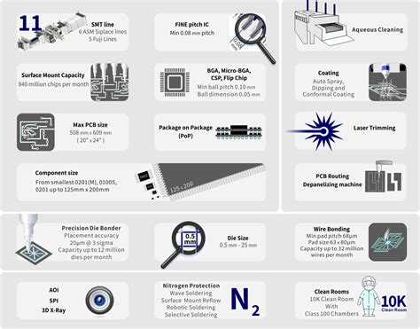
Modern PCB assembly processes are redefining electronics manufacturing through precision automation and data-driven optimization. By integrating advanced PCBA techniques, manufacturers achieve tighter tolerances (often within ±0.1mm) and error rates below 50ppm. Key innovations include:
| Technology | Impact | Example Applications |
|---|---|---|
| Robotic Soldering | Reduces human error by 90% | High-density interconnects |
| AOI Systems | Detects defects at 5μm resolution | Medical devices, aerospace systems |
| 3D Printed Circuits | Enables rapid prototyping (<24 hrs) | IoT sensors, wearable tech |
"The shift toward smart manufacturing in PCB assembly isn’t optional—it’s a baseline for competitiveness in Industry 4.0." – Industry Quality Analyst
Critical advancements like AI-driven inspection algorithms and modular assembly lines ensure scalability while maintaining rigorous quality control. For instance, thermal profiling during reflow soldering now leverages real-time analytics to prevent micro-cracking in assembled printed circuit boards.
Pro Tip:
Always validate PCBA designs against IPC-A-610 standards before full-scale production to minimize rework costs.
Emerging trends emphasize eco-friendly materials (e.g., halogen-free substrates) and energy-efficient processes, aligning with global sustainability mandates. By adopting these strategies, manufacturers not only elevate reliability but also accelerate time-to-market for next-generation electronics.
Advanced PCB Assembly Techniques
Modern electronics manufacturing relies on PCB assembly processes that blend precision engineering with cutting-edge technology. At the core of these advancements is precision automation, where robotic systems handle tasks like component placement, soldering, and inspection with micron-level accuracy. These automated workflows not only accelerate production but also minimize human error, ensuring consistency across high-volume PCBA (printed circuit board assembly) runs.
A key innovation driving this evolution is the integration of 3D printing for rapid prototyping of complex circuit designs. This enables manufacturers to test and refine layouts before full-scale production, reducing time-to-market for advanced electronics. Additionally, laser-direct imaging (LDI) systems optimize trace alignment, critical for high-frequency applications like 5G devices or IoT sensors.
To maintain reliability, PCB assembly workflows now incorporate automated optical inspection (AOI) and X-ray testing, which scrutinize solder joints and component alignment in real time. These quality assurance measures align with industry standards such as IPC-A-610, ensuring zero-defect output for mission-critical applications.
Emerging trends like smart manufacturing further enhance efficiency by leveraging IoT-enabled machinery and AI-driven analytics. These systems predict maintenance needs and adjust production parameters dynamically, minimizing downtime while optimizing resource use. Such advancements underscore how PCBA processes are redefining electronics manufacturing, balancing speed, precision, and sustainability in an increasingly connected world.
Precision Automation in PCB Manufacturing
Modern PCB assembly processes rely heavily on precision automation to meet the escalating demands of miniaturization and performance in electronics. Advanced robotic systems, such as automated optical inspection (AOI) and high-speed pick-and-place machines, ensure micron-level accuracy when positioning components on assembled printed circuit boards. These systems integrate machine vision and AI-driven algorithms to detect defects in real time, reducing human error and accelerating production cycles.
The shift toward PCBA (printed circuit board assembly) automation extends beyond component placement. Closed-loop feedback mechanisms enable dynamic adjustments during soldering and coating, maintaining consistent quality across high-volume batches. For instance, laser-guided systems achieve sub-100-micron alignment tolerances, critical for multilayer boards used in aerospace or medical devices.
Moreover, smart manufacturing frameworks connect PCB assembly lines with enterprise resource planning (ERP) platforms, enabling traceability from design to delivery. This synergy between hardware and software not only optimizes throughput but also supports just-in-time manufacturing principles. As industries push for faster time-to-market, the role of adaptive automation in PCBA will remain central to sustaining competitiveness while adhering to stringent quality benchmarks.
Next-Gen Solutions for Circuit Board Assembly
The evolution of PCB assembly processes is being driven by cutting-edge technologies that address the growing demands for miniaturization, performance, and sustainability. Modern AI-driven inspection systems now integrate machine learning algorithms to detect microscopic defects in PCBA with unparalleled accuracy, reducing error rates by up to 40% compared to traditional methods. Meanwhile, advancements in IoT-compatible assemblies enable real-time monitoring of assembled printed circuit boards during operation, ensuring proactive maintenance and extended product lifespans.
Additive manufacturing techniques, such as 3D-printed conductive traces, are redefining design flexibility, allowing engineers to create complex, high-density layouts previously deemed unachievable. Additionally, the adoption of modular assembly frameworks streamlines prototyping cycles, accelerating time-to-market for next-generation electronics. These innovations are further supported by eco-conscious materials like halogen-free substrates, aligning with global sustainability goals without compromising electrical performance.
To maintain seamless integration with smart manufacturing ecosystems, next-gen PCB assembly workflows now leverage cloud-based collaboration platforms. These systems enable cross-functional teams to optimize designs, simulate thermal dynamics, and validate signal integrity in virtual environments before physical production. By merging precision engineering with digital transformation, the industry is setting new benchmarks for reliability and efficiency in PCBA manufacturing.
Quality Control in Electronics PCB Assembly
Effective PCB assembly relies on rigorous quality control protocols to ensure reliability and performance in modern electronics. Advanced inspection systems, such as automated optical inspection (AOI) and X-ray imaging, detect microscopic defects like solder bridging or misaligned components during PCBA processes. These tools minimize human error while verifying compliance with design specifications. Additionally, environmental stress testing simulates extreme conditions—temperature fluctuations, vibration, and humidity—to validate board durability before deployment.
To maintain consistency, manufacturers implement statistical process control (SPC), analyzing production data in real time to identify deviations. This approach ensures that every assembled printed circuit board meets industry benchmarks like IPC-A-610 standards. Furthermore, traceability systems track components from sourcing to final assembly, addressing potential recalls efficiently.
Transitioning toward smart manufacturing, PCBA workflows now integrate machine learning algorithms to predict defects and optimize testing parameters. Such innovations not only elevate quality but also align with broader goals of precision automation and eco-friendly practices discussed in subsequent sections. By prioritizing these methodologies, the electronics industry continues to advance PCB assembly standards while reducing waste and operational costs.
Smart Manufacturing for Assembled PCBs
The integration of smart manufacturing into PCB assembly processes marks a transformative leap in electronics production. By leveraging IoT-enabled systems and AI-driven analytics, manufacturers now achieve unparalleled precision in monitoring PCBA workflows. Real-time data collection from sensors embedded in assembly lines enables proactive adjustments, minimizing defects and optimizing throughput. For instance, machine learning algorithms predict equipment maintenance needs, reducing unplanned downtime by up to 30% in advanced facilities.
Digital twin technology further enhances quality by simulating assembled printed circuit boards before physical production, identifying potential flaws in design or material compatibility. This synergy between virtual and physical systems ensures that PCB assembly adheres to strict tolerances while accelerating time-to-market. Automated optical inspection (AOI) systems, powered by high-resolution cameras and neural networks, now detect micron-level soldering anomalies with 99.8% accuracy—a critical advancement for industries like aerospace and medical devices.
As factories adopt adaptive manufacturing platforms, the flexibility to switch between PCBA designs without retooling becomes a reality. Such agility not only supports custom electronics demand but also aligns with sustainable practices by reducing material waste. By embedding intelligence at every stage, smart manufacturing elevates both the reliability and scalability of modern PCB assembly ecosystems.
Eco-Friendly Innovations in PCB Assembly
As environmental concerns intensify, the PCB assembly industry is prioritizing sustainable practices without compromising performance. A key advancement is the adoption of lead-free soldering techniques, which eliminate hazardous substances while maintaining robust electrical connections. Modern PCBA workflows now integrate halogen-free substrates and water-soluble flux formulations, reducing toxic waste during production.
Innovators are also leveraging recycling-compatible designs, enabling easier disassembly of assembled printed circuit boards for material recovery. Advanced facilities employ closed-loop systems to reclaim precious metals like copper and gold, cutting resource extraction by up to 40%. Additionally, energy-efficient PCB assembly lines powered by renewable sources are lowering carbon footprints—some factories report a 25% reduction in emissions through solar-powered reflow ovens.
Emerging bioplastics and biodegradable solder masks further minimize ecological impact, aligning with global e-waste regulations. These eco-conscious strategies not only meet stringent regulatory frameworks but also enhance brand credibility in markets demanding greener electronics. By embedding sustainability into PCBA processes, manufacturers are redefining industry benchmarks while addressing planetary stewardship.
Elevating Standards with Advanced PCBs
Modern PCB assembly processes are redefining quality benchmarks in electronics manufacturing by integrating precision engineering with smart automation. Advanced PCBA workflows now leverage robotic placement systems capable of handling components as small as 01005 packages, ensuring micron-level accuracy while minimizing human error. This shift not only accelerates production cycles but also enhances repeatability—a critical factor for industries like medical devices and aerospace, where component failure is not an option.
Beyond hardware advancements, data-driven quality assurance plays a pivotal role. Real-time optical inspection (AOI) and automated X-ray testing are now standard in PCB assembly lines, identifying defects like micro-cracks or soldering anomalies with sub-micron resolution. These protocols align with IPC-A-610 Class 3 specifications, guaranteeing reliability for mission-critical applications.
The adoption of flexible manufacturing systems further elevates standards, allowing seamless transitions between high-mix, low-volume PCBA projects and mass production. By combining modular assembly cells with IoT-enabled monitoring, manufacturers achieve unprecedented traceability—tracking every capacitor and resistor from placement to final testing. This convergence of precision automation and adaptive workflows positions modern PCB assembly as the backbone of next-generation electronics, setting new benchmarks for performance, scalability, and compliance.
Future Trends in Printed Circuit Board Assembly
The evolution of PCB assembly is accelerating as emerging technologies redefine manufacturing paradigms. A key trend lies in the integration of artificial intelligence (AI) and machine learning into PCBA workflows, enabling predictive maintenance and real-time defect detection. These systems analyze vast datasets to optimize solder paste application, component placement, and thermal management, significantly reducing error margins. Another transformative shift involves flexible hybrid electronics (FHE), combining rigid and stretchable substrates to support wearable tech and IoT devices.
As demand grows for miniaturized electronics, high-density interconnect (HDI) designs are becoming standard, requiring advanced laser drilling and microvia technologies. Simultaneously, sustainability pressures are driving innovations like biodegradable substrates and lead-free solder alloys in PCB assembly processes. The rise of 5G networks further intensifies the need for ultra-low-loss materials to maintain signal integrity in high-frequency applications.
Automation continues to dominate, with collaborative robots (cobots) now handling delicate tasks alongside human operators, enhancing precision without sacrificing scalability. These advancements, coupled with blockchain-enabled supply chain tracking, ensure transparency in PCBA sourcing and compliance. As these trends converge, they create a foundation for smarter, greener, and more resilient electronics manufacturing ecosystems.
Conclusion
The evolution of PCB assembly techniques underscores a transformative shift in electronics manufacturing, driven by precision automation and data-driven quality controls. As industries demand higher reliability in assembled printed circuit boards, the integration of smart manufacturing tools ensures seamless production workflows while minimizing human error. Innovations like AI-powered inspection systems and modular PCBA designs not only enhance scalability but also pave the way for adaptive manufacturing ecosystems.
Moreover, the emphasis on eco-friendly materials and energy-efficient processes reflects a growing alignment with global sustainability goals. By leveraging next-gen PCBA solutions, manufacturers can address rising complexity in circuit designs without compromising on speed or cost-efficiency. These advancements collectively elevate industry standards, ensuring assembled PCBs meet rigorous performance benchmarks across aerospace, medical, and consumer electronics sectors.
Looking ahead, the convergence of IoT-enabled monitoring and advanced soldering technologies will further refine production accuracy. As PCB assembly continues to evolve, its role as the backbone of modern electronics remains unchallenged—proving that innovation in manufacturing is not just about keeping pace but redefining what’s possible.
FAQs
What distinguishes advanced PCB assembly from traditional methods?
Advanced PCBA integrates precision automation and AI-driven systems, ensuring micron-level accuracy in component placement. This reduces human error and enhances throughput compared to manual processes.
How does quality control ensure reliability in assembled printed circuit boards?
Modern PCB assembly employs automated optical inspection (AOI) and X-ray testing to detect defects like solder bridges or misalignments. Statistical process control (SPC) further monitors production consistency, meeting IPC-A-610 standards.
Can smart manufacturing reduce lead times for PCBA projects?
Yes, IoT-enabled factories optimize real-time data from PCB assembly lines, enabling predictive maintenance and dynamic workflow adjustments. This slashes lead times by up to 30% while maintaining yield rates above 99%.
Are eco-friendly innovations compatible with high-performance assembled printed circuit boards?
Absolutely. Lead-free soldering, halogen-free substrates, and recyclable packaging are now standard in sustainable PCBA, balancing environmental compliance with thermal and electrical performance.
What future trends will shape PCB assembly technologies?
Embedded components, 3D-printed circuits, and quantum-dot soldering are emerging. These innovations will push assembled printed circuit boards toward higher density, faster signal transmission, and improved energy efficiency.
Ready to Elevate Your Electronics Manufacturing?
Explore cutting-edge PCB assembly solutions tailored to your needs. Please click here to discover how advanced PCBA can transform your production standards.