Streamlined HDI PCB Design for Efficient Electronics Manufacturing

Key Takeaways
When optimizing HDI PCB design for efficient electronics manufacturing, understanding core principles directly impacts pcb manufacturing cost and project timelines. Prioritizing microvia optimization reduces layer count while maintaining signal integrity—critical for compact layouts. Pairing this with high-frequency materials like Rogers 4350B ensures stable performance in RF applications, a key consideration for pcb manufacturing companies targeting aerospace or telecom sectors.
Integrating rigid-flex designs enables 3D packaging solutions, slashing assembly steps by up to 30% compared to traditional rigid boards. Tools like Altium Designer streamline stack-up planning, allowing you to simulate impedance control and thermal performance early in the design phase. This proactive approach minimizes revisions during pcb manufacturing, accelerating time-to-market.
| Technique | Cost Impact | Workflow Benefit |
|---|---|---|
| Microvia Optimization | Reduces layer count | Faster prototyping |
| Rigid-Flex Integration | Lowers assembly steps | Compact form factors |
| Altium Stack-Up Planning | Prevents late-stage changes | Improved yield rates |
By aligning design choices with pcb manufacturing business requirements—such as material selection and DFM checks—you avoid over-engineering while meeting performance benchmarks. For instance, specifying laser-drilled microvias instead of mechanical drilling cuts pcb manufacturing cost by 12–18% in high-density layouts. These strategies not only enhance reliability but also strengthen partnerships with pcb manufacturing companies by reducing their production complexities.
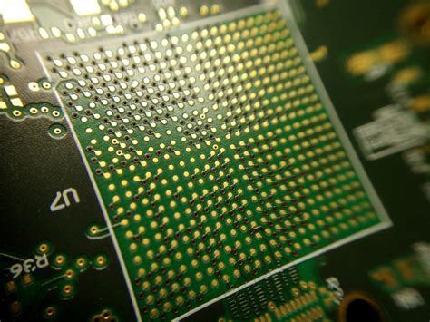
Microvia Optimization in HDI PCB Design
When designing high-density interconnect (HDI) PCBs, optimizing microvias is critical for balancing performance and PCB manufacturing cost. These laser-drilled structures enable tighter component placement by replacing through-hole vias, but their design requires precision. You’ll want to prioritize staggered or stacked microvia configurations based on signal integrity needs, as improper layouts can increase fabrication complexity. For instance, aspect ratios exceeding 6:1 risk plating voids, which may compromise reliability and escalate rework expenses for PCB manufacturing companies.
Tip: Use via-in-pad designs sparingly—while they save space, they demand advanced plating techniques to prevent solder wicking during assembly.
Collaborating early with your PCB manufacturing business partner ensures alignment on design-for-manufacturability (https://www.andwinpcba.com) help model thermal stress and impedance mismatches, ensuring microvias meet high-frequency demands without over-engineering. By streamlining these elements, you not only enhance signal integrity but also lower PCB manufacturing overheads through material efficiency and reduced scrap rates.
Remember, microvia optimization isn’t just about miniaturization—it’s a strategic lever to accelerate time-to-market while maintaining robustness in compact electronics.
High-Frequency Materials for Electronics Manufacturing
When selecting materials for PCB manufacturing in high-frequency applications, you need to prioritize substrates that minimize signal loss while maintaining thermal stability. Low dielectric loss laminates like Rogers RO4000® or PTFE-based composites are critical for high-speed circuits, as they reduce impedance mismatches and ensure consistent performance up to millimeter-wave frequencies. These materials directly influence PCB manufacturing cost, as their advanced properties often come at a premium—yet they enable thinner designs and fewer layers, offsetting expenses in complex assemblies.
For PCB manufacturing companies, balancing material performance with budget constraints requires careful analysis. High-frequency substrates like Isola’s Astra® MT77 or Nelco’s N7000-2HT® offer exceptional thermal conductivity, which simplifies heat dissipation in dense layouts. This reduces the need for additional cooling components, streamlining production workflows. However, integrating these materials demands precise fabrication techniques, as their softer structures can increase drill wear during microvia formation.
To optimize PCB manufacturing business outcomes, collaborate early with material suppliers and fabricators. Many high-frequency laminates require specialized handling, such as laser ablation for fine-pitch traces or plasma treatment for surface adhesion. Testing prototypes with controlled impedance structures ensures signal integrity before full-scale production, preventing costly redesigns. By aligning material choices with application-specific demands—whether for 5G infrastructure or aerospace systems—you achieve reliability without compromising scalability in high-volume manufacturing.
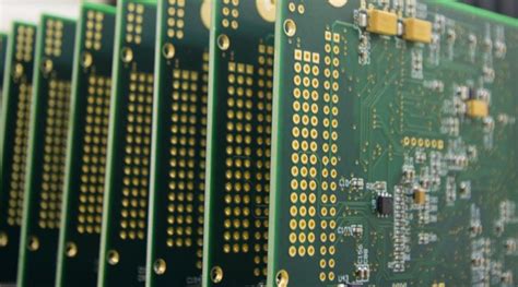
Rigid-Flex Integration in Compact PCB Layouts
When designing high-density interconnect (HDI) boards, rigid-flex integration becomes critical for balancing space constraints and functional complexity. By combining rigid and flexible substrates, you can achieve three-dimensional routing that bypasses traditional planar limitations, enabling tighter component placement in wearables, medical devices, or aerospace systems. This approach reduces reliance on bulky connectors and interposers, directly lowering PCB manufacturing cost through simplified assembly processes. However, transitioning to rigid-flex designs requires collaboration with experienced PCB manufacturing companies to optimize material selection (like polyimide flex layers) and avoid delamination risks during lamination.
To maintain cost efficiency, consider sequential build-up techniques that minimize layer counts while accommodating high-speed signals. Advanced PCB manufacturing business models now offer hybrid prototypes, allowing you to test rigid-flex layouts before full-scale production. Pay attention to z-height constraints and bend radius requirements early in the design phase—overlooking these can lead to rework expenses. Properly executed rigid-flex integration not only shrinks your board footprint but also enhances reliability in dynamic environments, making it a strategic advantage for competitive PCB manufacturing workflows.
Altium Tools for Streamlined HDI Design
When designing HDI PCBs, leveraging advanced software like Altium Designer ensures precision in managing complex layouts while aligning with PCB manufacturing requirements. The platform’s unified design environment simplifies layer stack-up planning, microvia placement, and high-density interconnects, directly addressing challenges faced by PCB manufacturing companies in producing compact, high-performance boards. By integrating automated design rule checks (DRCs), you reduce errors that could escalate PCB manufacturing cost during prototyping or mass production.
Altium’s 3D visualization tools enable real-time collaboration between design and manufacturing teams, ensuring rigid-flex integration aligns with mechanical constraints. Features like dynamic copper pour and differential pair routing optimize signal integrity, critical for high-frequency applications. For PCB manufacturing business models prioritizing speed, the software’s reusable template libraries accelerate design cycles by up to 30%, minimizing time-to-market.
Transitioning from design to production is seamless with Altium’s Gerber file generation and supply chain integration, which streamline communication with fabrication partners. This interoperability reduces misinterpretations, ensuring your HDI designs meet exact tolerances required for advanced PCB manufacturing processes. By balancing precision with efficiency, Altium tools bridge the gap between innovative HDI layouts and cost-effective manufacturability—key for scaling electronics production without compromising quality.
Cost-Effective HDI Manufacturing Strategies
To minimize pcb manufacturing cost without compromising quality, start by optimizing material selection. High-frequency laminates like Rogers 4350B offer performance benefits, but balancing dielectric properties with budget constraints is critical. Work closely with pcb manufacturing companies that provide tiered pricing for bulk orders or standardized panel sizes to reduce waste. For instance, using 18×24-inch panels instead of custom dimensions can lower material expenses by up to 12%.
Another strategy involves leveraging sequential lamination techniques to reduce layer counts in pcb manufacturing. By consolidating microvia layers and avoiding over-engineering, you streamline production while maintaining signal integrity. Advanced pcb manufacturing business partners often employ automated optical inspection (AOI) systems to catch defects early, preventing costly rework.
When designing for cost efficiency, prioritize DFM (Design for Manufacturing) checks in your HDI workflow. Tools like Altium’s ActiveBOM help identify component availability and pricing trends, enabling smarter sourcing decisions. Additionally, consider hybrid stack-ups that mix standard FR-4 with high-performance materials only where necessary—this approach can cut pcb manufacturing cost by 15–20% in high-density designs.
Finally, build long-term partnerships with pcb manufacturing companies specializing in HDI to negotiate volume pricing and faster turnaround times. Their expertise in process optimization, from laser-drilled microvias to controlled impedance routing, ensures you avoid hidden expenses while scaling production.

Accelerating Workflows With HDI Techniques
To stay competitive in modern PCB manufacturing, adopting high-density interconnect (HDI) techniques is essential for slashing production timelines. By integrating microvias and stacked via structures, you reduce the need for complex routing, enabling faster signal transmission and fewer design iterations. This directly lowers PCB manufacturing cost by minimizing material waste and rework cycles, a critical advantage for PCB manufacturing companies aiming to meet tight deadlines.
Advanced HDI workflows also simplify collaboration between design and fabrication teams. Tools like 3D modeling and automated design rule checks (DRCs) ensure manufacturability from the outset, preventing costly mid-process adjustments. For instance, optimizing via-in-pad designs early avoids delays during assembly—a common bottleneck in the PCB manufacturing business.
Additionally, HDI’s ability to support finer traces and smaller components allows for high-density layouts without sacrificing performance. This efficiency translates to fewer layers in multilayer boards, further trimming material expenses and assembly time. By prioritizing HDI-compatible materials and processes, you create a ripple effect: faster prototyping, smoother scaling, and ultimately, accelerated time-to-market—key metrics for thriving in today’s electronics sector.
Microvia Reliability in PCB Electronics
When designing high-density interconnect (HDI) boards, ensuring microvia reliability directly impacts the longevity and performance of your end product. Thermal cycling, mechanical stress, and electrochemical migration are critical factors that influence microvia durability. To mitigate risks, PCB manufacturing companies prioritize advanced laser drilling techniques paired with copper-filled via processes, which enhance structural integrity while minimizing voids.
Material selection plays a pivotal role—using low-CTE (coefficient of thermal expansion) substrates reduces stress on microvias during temperature fluctuations. This is particularly vital for applications requiring high-frequency signal integrity, where even minor defects can degrade performance. When optimizing PCB manufacturing cost, consider balancing advanced materials with streamlined fabrication steps—for instance, combining sequential lamination with laser ablation to reduce layer count without compromising reliability.
For PCB manufacturing business stakeholders, adopting design-for-manufacturability (DFM) guidelines ensures microvia aspect ratios stay within safe limits (typically ≤ 1:1 for stacked vias). Simulation tools like finite element analysis (FEA) help predict failure points early, avoiding costly rework. Finally, partnering with manufacturers certified in IPC-6012 Class 3 standards guarantees rigorous testing for microvia reliability, aligning your designs with industry benchmarks for mission-critical electronics.
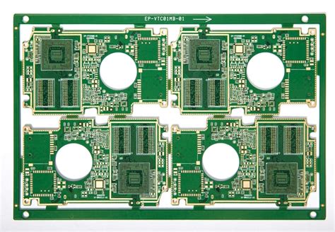
HDI Stack-Up Planning for Cost Control
Effective HDI stack-up planning directly impacts material utilization and process complexity, making it a critical lever for managing PCB manufacturing cost. When designing high-density interconnect boards, you’ll want to balance layer count with signal integrity requirements—each additional layer increases PCB manufacturing business expenses through material usage and lamination cycles. For example, opting for asymmetric stack-ups with buried or blind microvias can reduce sequential lamination steps, trimming both time and labor costs.
Collaborating early with PCB manufacturing companies ensures your stack-up aligns with their capabilities, avoiding costly redesigns. Prioritize dielectric materials that match your high-frequency needs while staying within budget—over-specifying substrates inflates PCB manufacturing costs without tangible performance gains. Additionally, consolidating power and ground layers minimizes via transitions, which lowers fabrication risks and improves yield.
By optimizing the stack-up for manufacturability, you streamline workflows for PCB manufacturing partners, reducing turnaround times and overhead. This approach not only controls expenses but also scales efficiently for high-volume production, making your designs more competitive in cost-sensitive markets.
Conclusion
As you refine your approach to HDI PCB design, the interplay between advanced techniques and PCB manufacturing efficiency becomes undeniable. By leveraging microvia optimization and high-frequency materials, you enable denser layouts without compromising signal integrity—directly translating to reduced PCB manufacturing cost and faster turnaround times. When paired with rigid-flex integration, these strategies empower PCB manufacturing companies to deliver compact, high-performance boards that meet evolving market demands.
Adopting tools like Altium for stack-up planning ensures seamless transitions from design to production, minimizing errors that could derail timelines. This precision becomes critical when scaling operations in a competitive PCB manufacturing business, where every design iteration impacts material waste and labor expenses. Remember: reliability isn’t just about component selection—it’s about designing for manufacturability from the start.
Ultimately, the synergy between intelligent HDI practices and collaboration with skilled PCB manufacturing partners creates a framework for sustainable growth. Whether you’re tackling high-frequency applications or space-constrained devices, prioritizing manufacturability in your design phase ensures your projects remain agile, cost-effective, and aligned with industry benchmarks.
FAQs
How does HDI PCB design affect manufacturing costs?
By optimizing microvia structures and stack-up configurations, you reduce layer counts and material waste. This directly lowers PCB manufacturing cost while maintaining signal integrity, making high-density designs more accessible for mid-volume production runs.
What should you prioritize when working with PCB manufacturing companies?
Ensure suppliers have traceability systems for high-frequency materials and rigid-flex integration capabilities. Reputable PCB manufacturing companies provide DFM feedback on via-in-pad tolerances and impedance control, preventing post-production delays.
Can HDI techniques accelerate prototyping cycles?
Yes. Using Altium’s HDI tools, you can automate annular ring checks and via-to-copper spacing rules. This slashes iteration time by 30-40%, allowing PCB manufacturing business partners to deliver functional prototypes within 5-7 business days.
How do thermal management practices differ in HDI designs?
With tighter component spacing, prioritize thermal relief patterns in microvia arrays and select materials with CTE matching. This prevents delamination during assembly, a critical factor for PCB manufacturing reliability in aerospace applications.
Ready to Optimize Your HDI Project?
Streamline your next design with manufacturers specializing in high-density solutions. Click here to request a feasibility analysis and cost breakdown tailored to your PCB manufacturing requirements.