Screen Printing for PCB Manufacturing: Techniques, Applications, and Advancements
Introduction to Screen Printing in PCB Fabrication
Screen printing, also known as silk screening, is a fundamental process in printed circuit board (PCB) manufacturing that has been used for decades to apply precise patterns of conductive and non-conductive materials onto substrate surfaces. This versatile printing technique remains essential in both prototype and mass production of PCBs, offering cost-effectiveness, reliability, and scalability.
In PCB fabrication, screen printing primarily serves three critical functions: applying solder mask layers, creating legend markings (component identifiers and polarity indicators), and depositing conductive traces in certain types of boards. While newer technologies like photolithography have replaced screen printing for some high-precision applications, the method continues to dominate many aspects of PCB production due to its simplicity, speed, and economic advantages for medium-feature-size requirements.
The Screen Printing Process: Step-by-Step
1. Screen Preparation
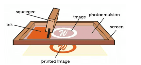
The screen printing process begins with the creation of the screen itself—a mesh frame that will control the deposition of ink onto the PCB substrate. Modern screens typically use stainless steel or polyester mesh with varying thread counts (usually between 90-400 threads per inch) depending on the required resolution. The mesh is stretched taut over an aluminum frame and coated with a light-sensitive emulsion.
2. Artwork and Stencil Creation
PCB designers create the artwork for the patterns to be printed using specialized CAD software. This design is then output to a high-resolution film positive. The emulsion-coated screen is exposed to UV light through this film positive, hardening the exposed areas while leaving the unexposed areas soluble. After development, the unexposed emulsion washes away, creating open areas in the mesh that correspond to the desired PCB pattern.
3. Ink Selection and Preparation
The choice of ink depends on the application:
- Conductive inks (containing silver, copper, or carbon) for trace deposition
- Solder mask inks (typically epoxy-based) for protective coatings
- Legend inks (usually epoxy or urethane-based) for component markings
Inks must be carefully formulated for proper viscosity, thixotropy (shear-thinning behavior), and curing characteristics.
4. Printing Process
The prepared screen is mounted in the screen printing machine above the PCB substrate. Ink is applied to the top of the screen, and a squeegee (typically polyurethane) moves across the screen with controlled pressure, forcing ink through the open mesh areas onto the board below. Key parameters include:
- Squeegee angle (usually 45-75°)
- Pressure (typically 0.5-2 kg/cm)
- Printing speed (commonly 10-30 cm/sec)
- Snap-off distance (gap between screen and substrate)
5. Curing and Post-Processing
After printing, the deposited ink must be cured. Thermal curing is most common, with temperatures ranging from 120-150°C for 15-60 minutes depending on the ink formulation. UV-curable inks offer faster processing times but may have different performance characteristics. Some processes may require multiple print-cure cycles for building thickness or printing different layers.
Technical Considerations in PCB Screen Printing
Resolution and Registration Accuracy
The resolution capability of screen printing is fundamentally limited by the mesh count and thread diameter. Typical minimum feature sizes are:
- Line width: 100-150 μm (4-6 mil) for standard processes
- Space between features: similar to line width
- Higher resolution screens can achieve 75 μm (3 mil) in optimized processes
Registration accuracy (alignment to existing board features) typically ranges from 50-100 μm (2-4 mil). Multi-color printing or multiple layer printing requires precise registration systems.
Ink Deposition Characteristics
Screen printing produces relatively thick deposits compared to other PCB patterning methods:
- Conductive traces: 10-25 μm dry thickness
- Solder mask: 15-40 μm dry thickness
- Legend printing: 10-20 μm dry thickness
The thickness can be controlled by mesh selection, emulsion thickness, and printing parameters. Multiple prints can build up additional thickness where needed.
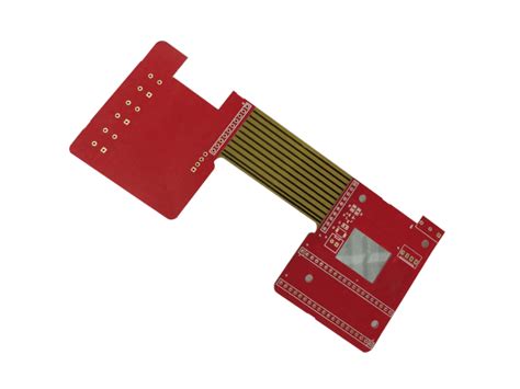
Substrate Considerations
Screen printing can be performed on various PCB substrates:
- FR-4 (most common)
- Flexible circuits (polyimide, PET)
- Ceramic substrates
- Metal-core boards
Each substrate requires consideration of surface energy, thermal expansion characteristics, and temperature sensitivity during curing.
Advantages of Screen Printing for PCB Manufacturing
Cost Effectiveness
Screen printing offers significant cost advantages over alternative methods:
- Lower equipment costs compared to photolithography or inkjet systems
- High throughput (hundreds to thousands of boards per hour)
- Minimal material waste
- Long screen life (thousands of impressions per screen)
Versatility
A single screen printing setup can handle:
- Multiple ink types (conductive, resistive, insulating)
- Various substrate sizes and shapes
- Different layer requirements (solder mask, legend, conductive patterns)
Material Flexibility
Screen printing accommodates a wide range of specialty inks:
- Thick-film conductive pastes (for higher current capacity)
- Resistive inks (for printed resistors)
- Dielectric inks (for multilayer boards)
- Specialty coatings (conformal coatings, adhesives)
Durability
Properly cured screen-printed layers offer:
- Excellent adhesion to substrates
- Good chemical resistance
- Mechanical durability
- Thermal stability for soldering processes
Limitations and Challenges
While screen printing is versatile, it does have limitations:
Resolution Constraints
The practical resolution limits make screen printing unsuitable for:
- High-density interconnect (HDI) boards
- Fine-pitch components (< 0.5 mm pitch)
- Microvia technologies
Process Control Requirements
Maintaining consistent print quality requires careful control of:
- Ink viscosity (affected by temperature, humidity, and age)
- Screen tension (changes with use)
- Squeegee wear
- Environmental conditions
Artwork Modification Challenges
Design changes require new screens, which involves:
- Additional costs for new screens
- Lead time for screen production
- Potential registration issues with existing screens
Recent Technological Advancements
Improved Materials
Advanced Meshes:
- Ultra-thin stainless steel meshes for higher resolution
- Composite meshes for improved durability
- Nanocoated meshes for better ink release
Enhanced Inks:
- Conductive inks with improved conductivity and adhesion
- Low-temperature cure inks for heat-sensitive substrates
- Environmentally friendly formulations with reduced VOCs
Automation and Process Control
Modern screen printing systems incorporate:
- Automated vision systems for registration
- Closed-loop viscosity control
- Real-time print quality monitoring
- Automated screen cleaning and maintenance
Hybrid Approaches
Combining screen printing with other technologies:
- Screen printing base layers with inkjet for fine features
- Using screen printing for bulk deposition followed by laser ablation for precision
- Combining screen printed conductors with plated through holes
Applications in PCB Manufacturing
Solder Mask Application
Screen printing remains a dominant method for solder mask application, particularly:
- For larger feature sizes
- In high-volume production
- When cost is a primary consideration
Legend Printing
Component identification markings are almost exclusively screen printed due to:
- Durability requirements
- Color options (typically white, but other colors available)
- Cost-effectiveness
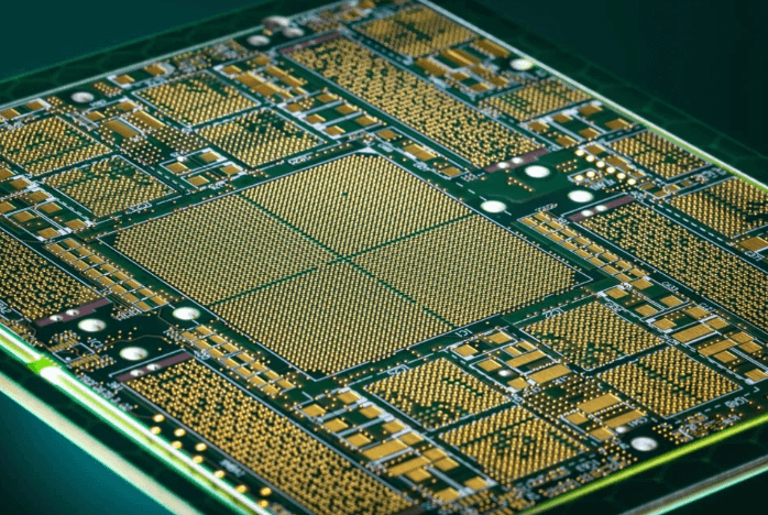
Thick-Film Circuits
Screen printing is essential for:
- Ceramic PCBs
- Hybrid circuits
- Power electronics with thick conductors
- Printed resistors and capacitors
Membrane Switches
Flexible membrane switches rely on screen printing for:
- Conductive traces
- Graphic overlays
- Adhesive layers
Quality Control and Testing
Effective quality control in PCB screen printing involves:
Visual Inspection
- Checking for complete pattern transfer
- Verifying absence of pinholes or voids
- Ensuring proper edge definition
Dimensional Verification
- Measuring line widths and spaces
- Checking registration to other layers
- Verifying thickness of deposits
Performance Testing
- Adhesion testing (tape tests, cross-hatch)
- Electrical continuity testing for conductive patterns
- Solderability testing for solder mask applications
- Cure verification (MEK rub tests, infrared analysis)
Environmental and Safety Considerations
Material Handling
- Proper storage of inks (temperature control, shelf life monitoring)
- Safe handling of solvents and cleaners
- Prevention of ink skin formation (through proper container sealing)
Waste Management
- Recycling of screen materials
- Proper disposal of used inks and cleaners
- Recovery and reuse of excess ink where possible
Workplace Safety
- Adequate ventilation for solvent vapors
- Protective equipment for operators (gloves, eye protection)
- Ergonomic considerations for repetitive motions
Future Outlook
While alternative technologies continue to advance, screen printing is expected to maintain its position in PCB manufacturing due to:
Continued Material Developments
- Nano-particle inks for better conductivity at lower temperatures
- Improved environmentally friendly formulations
- Specialty inks for emerging applications (flexible electronics, wearable devices)
Process Improvements
- Higher precision automation
- Better integration with other manufacturing steps
- Advanced process monitoring and control systems
New Applications
- Printed electronics
- RFID antennas
- Flexible hybrid electronics
- Internet of Things (IoT) devices
Conclusion
Screen printing remains a vital technology in PCB manufacturing, offering an optimal balance of cost, quality, and throughput for many applications. While it may not satisfy the most demanding high-density interconnect requirements, its versatility, material flexibility, and economic advantages ensure its continued relevance in both conventional and emerging electronic applications. As materials and processes continue to evolve, screen printing will adapt to maintain its position as a fundamental PCB fabrication technology, particularly for solder mask application, legend printing, and thick-film circuit production.
The future of screen printing in PCB manufacturing lies in its integration with newer technologies, creating hybrid approaches that leverage the strengths of multiple processes. By combining the bulk deposition capabilities of screen printing with the precision of digital methods, manufacturers can achieve optimal results across a wide range of product requirements. As the electronics industry continues to demand both performance and cost-effectiveness, screen printing’s role in PCB fabrication appears secure for the foreseeable future.