Expert HDI PCB Manufacturing Solutions for Advanced Applications

Key Takeaways
When selecting PCB manufacturing partners for advanced applications, understanding core competencies becomes crucial. Leading PCB manufacturing companies leverage microvia technology and laser drilling to achieve trace densities exceeding 20 lines/cm, enabling miniaturized designs without compromising performance. For industries like aerospace or medical tech, PCB manufacturing cost optimization often hinges on material selection and layer count—choosing low-loss substrates or sequential lamination can reduce expenses by up to 30% while maintaining reliability.
"Always verify compliance with IPC-2226 standards during design reviews—this ensures your HDI boards meet thermal and mechanical stress requirements for mission-critical systems."
A well-structured PCB manufacturing business prioritizes automated optical inspection (AOI) and electrical testing to minimize defects in high-density layouts. Advanced facilities also employ any-layer buildup processes, which eliminate the need for mechanical drilling in ultra-thin designs. By aligning your project’s complexity with a manufacturer’s technical capabilities, you avoid over-engineering and reduce turnaround times. Transitioning to HDI solutions doesn’t just save space—it future-proofs your product against evolving performance demands in sectors like 5G infrastructure or wearable tech.
HDI PCB Manufacturing for Medical Devices
When designing medical devices, you need PCB manufacturing solutions that prioritize precision, reliability, and compliance. Medical applications demand boards capable of supporting high-frequency signals, miniaturized components, and rigorous sterilization processes. Leading PCB manufacturing companies leverage high-density interconnect (HDI) technology to achieve tighter trace spacing and microvia architectures, ensuring optimal performance in devices like implantable monitors, imaging systems, and portable diagnostics.
A critical factor in PCB manufacturing cost for medical projects is material selection. High-frequency laminates and biocompatible substrates are often required to meet regulatory standards, such as ISO 13485. Advanced laser drilling and sequential lamination processes enable the creation of ultra-fine circuits, reducing signal loss and improving durability—key for life-critical applications. For instance, medical-grade HDI boards often incorporate blind/buried vias to maximize space efficiency without compromising functionality.
Balancing PCB manufacturing business priorities—like scalability and lead times—with strict quality controls is essential. Partnering with manufacturers experienced in IPC-2226 standards ensures your designs meet both technical and regulatory requirements. By optimizing layer counts and via structures, you can achieve cost-efficiency while maintaining the integrity needed for medical environments. This approach not only streamlines production but also future-proofs devices against evolving healthcare technologies.
Aerospace-Grade HDI Circuit Solutions
When designing mission-critical systems for aerospace applications, you need HDI PCB manufacturing solutions that prioritize reliability under extreme conditions. Aerospace-grade circuits demand ultra-precise layering, advanced material selection, and rigorous testing to withstand temperature fluctuations, vibration, and radiation exposure. Leading PCB manufacturing companies leverage microvia technology and sequential lamination processes to achieve sub-15μm trace widths, ensuring signal integrity in compact, high-density designs.
Balancing PCB manufacturing cost with performance is critical, as aerospace projects often involve low-volume, high-complexity boards. By partnering with specialists in the PCB manufacturing business, you gain access to materials like polyimide or ceramic-filled substrates that enhance thermal stability without compromising weight constraints. These providers adhere to MIL-PRF-31032 and AS9100 standards, guaranteeing traceability and compliance for avionics, satellite systems, and navigation equipment.
Transitioning from medical or consumer tech applications? Aerospace HDI solutions require additional validation cycles, including thermal shock testing and cross-sectional analysis. This ensures boards maintain functionality in environments where failure isn’t an option. By optimizing layer stack-ups and via structures early in the design phase, you minimize rework and align with stringent aerospace timelines.
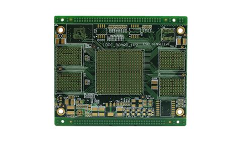
Microvia Technology in HDI Production
When implementing HDI PCB manufacturing, microvia technology becomes critical for achieving the mini-density requirements of modern electronics. Unlike traditional through-hole vias, microvias—typically defined as holes with diameters below 150 microns—enable PCB manufacturing companies to create intricate multilayer designs while conserving space. These laser-drilled structures allow for stacked or staggered via configurations, enhancing signal integrity in high-frequency applications like 5G modules or IoT devices.
A key advantage lies in reducing PCB manufacturing cost. By using microvias, designers can minimize layer counts and material usage without compromising performance. For example, replacing a 12-layer board with an 8-layer HDI design using microvias can lower production expenses by up to 20%, while maintaining reliability standards like IPC-2226. Below is a comparison of microvia benefits:
| Feature | Microvia Technology | Traditional Through-Holes |
|---|---|---|
| Diameter Range | 50–150 μm | 200–500 μm |
| Layer Efficiency | 30% higher | Standard |
| Signal Loss | <0.5 dB/inch | >1.2 dB/inch |
This approach also supports the PCB manufacturing business by enabling faster prototyping cycles. Advanced laser systems ensure precision down to ±10 μm, critical for aerospace sensors or medical imaging equipment. However, balancing thermal management and via fill quality remains essential to avoid reliability issues in extreme environments. By integrating microvias into your designs, you unlock scalable solutions for shrinking form factors and rising performance demands.
Cost-Effective HDI PCB Fabrication
Achieving cost efficiency in PCB manufacturing requires balancing advanced technical capabilities with strategic material and process optimization. When selecting PCB manufacturing companies for high-density interconnect (HDI) boards, you need partners who streamline production without compromising on layer stacking precision or microvia reliability. Laser drilling and sequential lamination techniques, for instance, minimize material waste while maintaining tight tolerances—critical for reducing PCB manufacturing cost in complex designs.
Forward-thinking PCB manufacturing business models leverage economies of scale through automated optical inspection (AOI) and standardized testing protocols, which cut downtime and rework expenses. By optimizing panel utilization and adopting thinner dielectric materials, manufacturers can lower raw material costs by up to 20% without sacrificing signal integrity. Additionally, partnering with facilities that offer volume pricing tiers ensures scalability for high-mix, low-volume projects common in aerospace or medical sectors.
However, cost-effectiveness shouldn’t come at the expense of compliance. Reputable providers align their processes with IPC-2226 standards to guarantee thermal stability and electrical performance, even in ultra-thin designs. This approach not only reduces long-term failure risks but also aligns with lifecycle cost calculations—a key consideration when evaluating PCB manufacturing partnerships for mission-critical applications.
IPC-2226 Compliant HDI Boards
When selecting PCB manufacturing companies for high-density interconnect (HDI) boards, compliance with IPC-2226 standards becomes critical. These guidelines ensure that HDI PCB manufacturing processes meet rigorous requirements for layer alignment, material integrity, and thermal management—factors that directly impact performance in advanced applications like aerospace or medical systems. For instance, microvia reliability and signal integrity depend on adherence to these specifications, which dictate everything from dielectric thickness to copper plating uniformity.
Understanding PCB manufacturing cost drivers is essential when designing IPC-2226-compliant boards. While tighter tolerances and specialized materials may increase initial expenses, they reduce long-term risks like field failures or redesigns. Reputable PCB manufacturing business partners optimize this balance by leveraging advanced laser drilling and sequential lamination techniques, ensuring compliance without unnecessary overhead. This alignment with industry standards also simplifies certification processes, particularly for sectors where traceability and quality documentation are non-negotiable.
By prioritizing IPC-2226 compliance, you ensure that your HDI boards deliver consistent performance under extreme conditions—whether in low-earth orbit satellites or implantable medical devices. Partnering with manufacturers who integrate these standards into their PCB manufacturing workflows guarantees that your designs meet both technical and regulatory expectations seamlessly.
High-Density PCBs for Consumer Tech
As consumer electronics shrink in size while demanding higher performance, PCB manufacturing processes must adapt to meet these dual challenges. Modern devices like smartphones, wearables, and IoT gadgets rely on high-density interconnect (HDI) designs to integrate complex circuitry into compact form factors. Leading PCB manufacturing companies leverage laser-drilled microvias and stacked via structures to achieve trace widths under 40µm, enabling faster signal transmission and reduced electromagnetic interference—critical for 5G and AI-driven applications.
Balancing PCB manufacturing cost with quality remains a priority, especially for high-volume consumer products. Advanced HDI techniques, such as sequential lamination and via-in-pad plating, minimize material waste while ensuring reliability. However, optimizing PCB manufacturing business workflows—from design validation to testing—requires collaboration with partners who understand thermal management and impedance control for high-frequency operations.
When selecting a manufacturer, verify their expertise in IPC-2226 standards and their ability to scale production without compromising precision. As consumer expectations evolve, partnering with innovators in HDI PCB manufacturing ensures your products stay ahead in performance, durability, and cost-efficiency.
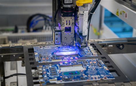
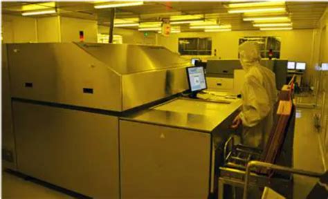
Advanced HDI Manufacturing Facilities
When selecting a partner for PCB manufacturing, the capabilities of their production facilities directly impact the quality and reliability of your high-density interconnect boards. Leading PCB manufacturing companies invest in state-of-the-art equipment, including laser direct imaging (LDI) systems and automated optical inspection (AOI), to ensure precision in microvia formation and layer alignment. These technologies enable the creation of ultra-fine traces and stacked vias, critical for advanced applications like medical implants or aerospace avionics.
Modern PCB manufacturing cost optimization relies on facilities equipped with advanced plating lines and vacuum lamination presses, which reduce material waste while maintaining IPC-2226 compliance. For businesses managing a PCB manufacturing business, partnering with a manufacturer that utilizes robotic assembly lines and real-time process monitoring ensures consistent yields, even for designs requiring 20+ layers or hybrid materials. Transitioning seamlessly from prototyping to mass production, such facilities balance technical rigor with scalability—key for industries where design complexity and time-to-market pressures intersect. By integrating environmental controls and lean manufacturing principles, top-tier providers deliver high-reliability solutions without compromising on turnaround times or cost efficiency.
Reliable HDI Solutions for Aerospace
When designing systems for aerospace applications, you need HDI PCBs that withstand extreme conditions while maintaining signal integrity. High-density interconnect technology enables compact layouts critical for avionics, satellite communications, and navigation systems, where weight reduction and thermal stability are non-negotiable. Leading PCB manufacturing companies prioritize materials like polyimide or ceramic-based substrates to handle rapid temperature fluctuations and mechanical stress, ensuring compliance with MIL-PRF-31032 and other aerospace standards.
Balancing PCB manufacturing cost with performance requires expertise in optimizing layer counts, microvia configurations, and impedance control. Advanced PCB manufacturing business practices, such as automated optical inspection (AOI) and cross-sectional analysis, minimize defects in high-layer-count designs. By partnering with manufacturers experienced in low-Dk/Df materials and sequential lamination, you achieve reliability without compromising on signal speed or power distribution—key factors for mission-critical aerospace electronics. Transitioning to these solutions ensures your designs meet both technical demands and stringent certification requirements.
Conclusion
When selecting partners for PCB manufacturing, it’s critical to evaluate PCB manufacturing companies based on their ability to balance technical expertise with cost efficiency. Advanced applications demand precision in design and compliance with standards like IPC-2226, which directly impacts PCB manufacturing cost and long-term reliability. By prioritizing suppliers with proven microvia technology and aerospace-grade quality controls, you ensure your high-density boards meet stringent performance requirements without compromising scalability.
For businesses navigating the complexities of PCB manufacturing business, partnering with facilities that integrate automated processes and rigorous testing protocols reduces risks in high-stakes industries like medical or aerospace. Cost-effective solutions don’t mean cutting corners—they require strategic material selection and optimized production workflows. Ultimately, the right manufacturer becomes an extension of your engineering team, delivering reliable solutions that align with both technical specifications and budgetary constraints.
FAQs
What distinguishes HDI PCBs from standard PCBs in pcb manufacturing?
HDI PCBs use advanced microvia technology and higher wiring density, enabling compact designs critical for medical and aerospace applications. Unlike standard boards, they prioritize precision layering and laser-drilled vias to meet strict IPC-2226 standards.
How do pcb manufacturing companies ensure reliability for aerospace applications?
Top manufacturers implement rigorous testing protocols, including thermal cycling and signal integrity checks. Aerospace-grade HDI boards often incorporate specialized materials like polyimide to withstand extreme conditions while maintaining signal performance.
What factors influence pcb manufacturing cost for high-density designs?
Cost depends on layer count, material selection, and microvia complexity. While advanced features like blind/buried vias increase expenses, partnering with experienced pcb manufacturing business providers optimizes budgets through scalable production and design-for-manufacturability (DFM) guidance.
Why is IPC-2226 compliance critical in HDI pcb manufacturing?
This standard ensures boards meet performance benchmarks for high-frequency applications, such as 5G devices or medical imaging systems. Compliance guarantees proper spacing, via placement, and material integrity, reducing failure risks in mission-critical environments.
Can HDI technology reduce long-term costs in consumer electronics?
Yes. By enabling smaller, lighter designs with fewer connectors, HDI PCBs lower assembly costs and improve product longevity. Leading pcb manufacturing companies leverage automated processes to further streamline production for high-volume orders.
Explore Our HDI PCB Manufacturing Solutions
For tailored high-density circuit solutions, please click here: https://www.andwinpcb.com/pcb-manufacturing/. Our team specializes in balancing performance demands with cost-effective fabrication for advanced applications.