The Importance and Design Considerations of PCB Ground Planes
Introduction to PCB Ground Planes
In modern printed circuit board (PCB) design, the ground plane represents one of the most critical elements that can make or break the performance of an electronic device. A ground plane is a large area of copper on a PCB layer that serves as a common reference point for electrical circuits, providing both signal return paths and shielding against electromagnetic interference (EMI). This article explores the multifaceted role of ground planes in PCB design, examining their various types, implementation strategies, and best practices for optimal performance.
Fundamental Concepts of Ground Planes
Electrical Characteristics
The ground plane in a PCB serves as a low-impedance return path for electrical currents, maintaining a stable reference voltage throughout the system. Its effectiveness stems from several key electrical properties:
- Low Impedance: The large copper area offers minimal resistance to current flow
- Capacitance: Forms distributed capacitance with adjacent layers and traces
- Inductance: Provides lower inductance return paths compared to thin traces
Physical Implementation
Ground planes typically occupy entire layers of multilayer PCBs or significant portions of single-layer boards. They can be implemented as:
- Solid copper pours
- Hatched patterns (less common in modern designs)
- Segmented areas for different ground types (with careful consideration)
Types of Ground Plane Configurations
Single-Layer Ground Planes
In simpler single or double-layer boards, ground planes often share space with signal traces:
- Typically cover all unused board area
- May require more creative routing to maintain continuity
- Often supplemented with ground grids or pour fill areas
Multilayer Ground Planes
Modern high-speed designs commonly use dedicated ground plane layers:
- Single Ground Plane: One complete layer serving as reference
- Multiple Ground Planes: Separate layers for different circuit sections
- Ground/Power Plane Pairs: Adjacent ground and power layers for capacitance
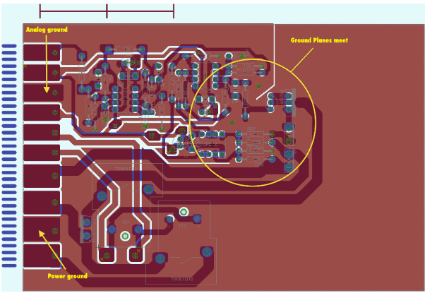
Split Ground Planes
Some designs partition ground planes for different purposes:
- Analog/Digital Separation: Prevents noise coupling between domains
- Power Ground Separation: Isolates high-current return paths
- RF/Baseband Partitioning: Maintains signal integrity in mixed-signal systems
Key Benefits of Proper Ground Plane Implementation
Signal Integrity Enhancement
- Controlled Impedance: Provides consistent reference for transmission lines
- Reduced Crosstalk: Shields adjacent signals from mutual interference
- Minimized Ground Bounce: Low-impedance path prevents voltage fluctuations
EMI Reduction
- Shielding: Acts as barrier to radiated emissions
- Current Return Path Management: Contains electromagnetic fields
- Common-Mode Noise Suppression: Reduces antenna-like radiation effects
Thermal Management
- Heat Dissipation: Large copper areas spread thermal energy
- Component Cooling: Provides thermal relief for heat-generating parts
- Temperature Stabilization: Helps maintain uniform board temperature
Design Considerations for Optimal Ground Planes
Layer Stackup Planning
- Proximity to Signal Layers: Critical for high-speed designs
- Symmetry: Balances mechanical stress and warpage
- Dielectric Material Selection: Affects impedance and capacitance
Ground Plane Continuity
- Minimizing Splits: Preserves low-impedance characteristics
- Strategic Segmentation: When necessary for noise isolation
- Via Placement: Ensures proper connection between layers
Mixed-Signal Grounding Strategies
- Single-Point Grounding: For low-frequency analog circuits
- Multipoint Grounding: Preferred for high-speed digital systems
- Hybrid Approaches: Combining techniques for mixed-signal boards
Common Ground Plane Pitfalls and Solutions
Ground Loops
Problem: Multiple return paths creating noise-inducing loops
Solution: Careful topology planning and single-point grounding where appropriate
Split Plane Resonance
Problem: Cavity resonance in partitioned ground areas
Solution: Strategic placement of stitching capacitors or vias
Insufficient Via Connections
Problem: High impedance between ground layers
Solution: Adequate via stitching with proper spacing (typically λ/20)
Over-Segmentation
Problem: Excessive splitting compromising plane effectiveness
Solution: Only split when absolutely necessary for noise isolation
Advanced Ground Plane Techniques
Embedded Ground Planes
- Buried Layers: Internal ground planes in high-layer-count PCBs
- Localized Ground Islands: Small ground areas under sensitive components
Ground Plane Shaping
- Contoured Edges: For impedance control at board edges
- Moats and Bridges: For controlled separation of ground regions
- Thermal Relief Patterns: For component pads to prevent soldering issues
High-Speed Design Considerations
- Return Path Management: Ensuring continuous paths beneath signals
- Via Transitions: Minimizing discontinuities at layer changes
- Edge Rate Control: Matching ground plane performance to signal speeds
Manufacturing and Practical Considerations
Fabrication Tolerances
- Copper Thickness: Affects current-carrying capacity
- Etching Precision: Impacts minimum clearance requirements
- Surface Finishes: Influence solderability and corrosion resistance
Assembly Factors
- Thermal Relief: Preventing heat sinking during soldering
- Test Point Access: Ensuring ground accessibility for debugging
- Rework Considerations: Facilitating component replacement
Cost Optimization
- Layer Count Reduction: Balancing performance with budget
- Material Selection: Choosing appropriate dielectric materials
- Manufacturability: Designing for high yield and reliability
Verification and Testing Methods
Pre-Layout Analysis
- Stackup Modeling: Predicting impedance characteristics
- Signal Integrity Simulation: Anticipating performance issues
- Thermal Modeling: Evaluating heat dissipation capability
Post-Layout Verification
- Design Rule Checking (DRC): Ensuring manufacturing compliance
- Electromagnetic Simulation: Predicting EMI performance
- Power Integrity Analysis: Verifying ground network adequacy
Physical Testing
- Impedance Measurement: Verifying transmission line performance
- Ground Continuity Testing: Ensuring low-resistance paths
- EMI Scanning: Identifying radiation hotspots
Future Trends in Ground Plane Technology
3D Printed Electronics
- Conformal Ground Layers: Adapting to non-planar surfaces
- Graded Material Properties: Transitioning impedance gradually
Advanced Materials
- Graphene-Based Planes: For ultra-high conductivity
- Metamaterial Surfaces: Engineered electromagnetic properties
Intelligent Ground Systems
- Active Ground Plane Control: Adaptive impedance matching
- Self-Monitoring Grounds: Embedded sensors for real-time analysis
Conclusion
The PCB ground plane remains a fundamental element in electronic design, growing more sophisticated as technology advances. Proper implementation requires balancing electrical requirements, manufacturing constraints, and cost considerations. By understanding the principles outlined in this article, designers can create ground systems that optimize signal integrity, minimize EMI, and ensure reliable operation across increasingly demanding applications. As electronic systems continue to push performance boundaries, innovative ground plane strategies will remain essential for meeting tomorrow’s design challenges.