Network PCB: Design, Applications, and Future Trends
1. Introduction
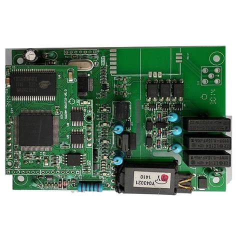
Printed Circuit Boards (PCBs) are the backbone of modern electronics, providing mechanical support and electrical connections for components. Among the various types of PCBs, Network PCBs play a crucial role in communication systems, networking hardware, and high-speed data transmission. These specialized PCBs are designed to handle high-frequency signals, minimize interference, and ensure reliable connectivity in devices such as routers, switches, servers, and IoT (Internet of Things) systems.
This article explores the design considerations, materials, applications, and future trends of Network PCBs, providing insights into their importance in today’s interconnected world.
2. Key Design Considerations for Network PCBs
Designing a Network PCB requires careful attention to signal integrity, power distribution, and thermal management. Below are the primary considerations:
2.1 Signal Integrity and High-Speed Design
Network PCBs often operate at high frequencies, making signal integrity a critical factor. Key aspects include:
- Impedance Control: Maintaining consistent impedance (typically 50Ω or 100Ω for differential pairs) to prevent signal reflections.
- Crosstalk Mitigation: Proper spacing between traces and the use of ground planes to reduce electromagnetic interference (EMI).
- Differential Pair Routing: Essential for high-speed interfaces like Ethernet, USB, and PCIe to ensure noise immunity.
2.2 Layer Stackup and Material Selection
The choice of PCB materials and layer stackup impacts performance:
- High-Frequency Laminates: Materials like Rogers, Isola, or FR-4 with low dielectric loss (Df) are preferred for minimizing signal attenuation.
- Multilayer PCBs: Typically 4 to 12 layers, with dedicated signal, power, and ground layers to reduce noise.
- Controlled Dielectric Constant (Dk): Ensures consistent signal propagation speed.
2.3 Power Integrity and Thermal Management
- Decoupling Capacitors: Placed near ICs to stabilize power supply and reduce noise.
- Thermal Vias & Heat Sinks: Used to dissipate heat from high-power components like processors and RF modules.
- Power Plane Segmentation: Prevents voltage drops and ensures stable power delivery.
2.4 EMI/EMC Compliance
Network devices must comply with electromagnetic interference (EMI) and electromagnetic compatibility (EMC) standards. Techniques include:
- Shielding: Using metal cans or conductive coatings to block interference.
- Proper Grounding: Star grounding or multi-point grounding to minimize noise.
- Filtering: Ferrite beads and LC filters to suppress high-frequency noise.
3. Applications of Network PCBs
Network PCBs are integral to various communication and computing systems:
3.1 Networking Hardware
- Routers & Switches: High-speed PCBs with multiple Ethernet ports and signal conditioning circuits.
- Network Interface Cards (NICs): Enable wired/wireless connectivity in computers.
- Optical Transceivers: Used in fiber-optic communication with high-frequency PCBs.
3.2 Data Centers & Servers
- Server Motherboards: Require high-layer-count PCBs with optimized power delivery.
- Storage Area Networks (SANs): High-speed interconnects like NVMe over Fabrics (NVMe-oF).
3.3 Wireless Communication
- 5G Base Stations: RF PCBs with millimeter-wave support.
- Wi-Fi 6/6E Modules: High-frequency PCBs for low-latency communication.
3.4 IoT & Edge Computing
- Smart Devices: Network-enabled sensors and gateways.
- Industrial IoT (IIoT): Ruggedized PCBs for harsh environments.
4. Advanced Technologies in Network PCBs
4.1 High-Density Interconnect (HDI) PCBs
- Microvias & Blind/Buried Vias: Enable compact designs with higher routing density.
- Fine-Pitch Components: Supports miniaturization in networking devices.
4.2 Embedded Components
- Passive Components (Resistors, Capacitors): Embedded within the PCB to save space.
- Active Components (ICs): Emerging technology for ultra-compact designs.
4.3 Flexible & Rigid-Flex PCBs
- Used in wearable networking devices and compact IoT modules.
4.4 AI-Optimized PCBs
- Machine learning-assisted PCB design for optimal routing and signal integrity.
5. Future Trends in Network PCB Design
5.1 Higher Speeds (Beyond 100G Ethernet)
- 112G/224G SerDes: Demands advanced materials and signal conditioning techniques.
- Photonics Integration: Optical PCBs for ultra-high-speed data centers.
5.2 Sustainable PCB Manufacturing
- Lead-Free & Halogen-Free Materials: Eco-friendly alternatives.
- Recyclable Substrates: Reducing e-waste.
5.3 3D-Printed Electronics
- Additive manufacturing for rapid prototyping of network PCBs.
5.4 Quantum Networking
- Emerging PCB designs for quantum communication systems.
6. Conclusion
Network PCBs are at the heart of modern communication systems, enabling high-speed data transfer, reliable connectivity, and advanced computing. As networking technology evolves—driven by 5G, AI, and IoT—PCB design must adapt to meet higher performance demands. Innovations in materials, manufacturing, and signal integrity will shape the future of Network PCBs, ensuring faster, more efficient, and sustainable electronic systems.
By understanding the design principles and emerging trends, engineers can develop next-generation Network PCBs that power the connected world.