Precision Engineering for High Volume PCB Projects
Key Takeaways
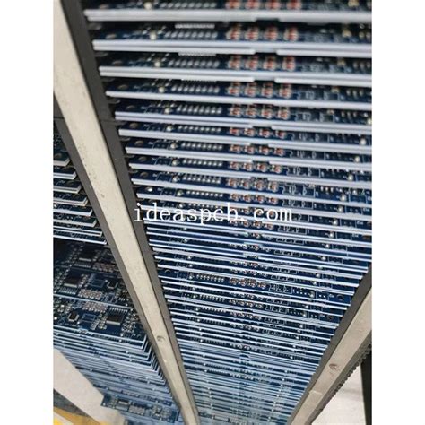
When managing PCB manufacturing at scale, you need solutions that balance speed with precision. Modern PCB manufacturing companies rely on advanced depaneling systems to maintain component integrity while processing thousands of boards. For example, laser-based depaneling minimizes stress on delicate circuits, reducing the risk of microcracks—a critical factor when PCB manufacturing cost optimization depends on minimizing waste.
To meet IPC-compliant microsectioning standards, automated optical inspection (AOI) systems verify solder joints and layer alignment, ensuring every batch adheres to industry benchmarks. This is non-negotiable for PCB manufacturing business models targeting aerospace or medical sectors, where reliability directly impacts regulatory approvals.
| Factor | Manual Depaneling | Automated Depaneling |
|---|---|---|
| Throughput | 50-100 boards/hr | 500-1,000 boards/hr |
| Defect Rate | 1.2% | 0.3% |
| Scalability | Limited | High |
Tip: Integrate depaneling and testing phases to catch defects early, reducing rework costs by up to 40% in high-volume runs.
For workflows to scale, prioritize systems that sync with pick-and-place machines and conveyors. Tools like IPC-certified microsection analysis ensure traceability, which is vital when auditing supply chains. By aligning your processes with these strategies, you’ll not only meet demand but future-proof your production against evolving quality thresholds.
PCB Depaneling Systems for High Volumes
When scaling PCB manufacturing operations, selecting the right depaneling system directly impacts efficiency and product reliability. High-volume projects demand equipment that balances speed with precision, as even minor errors in separating boards can compromise component integrity or escalate PCB manufacturing costs. Modern depaneling systems leverage laser cutting or advanced router-based methods to minimize stress on delicate traces, ensuring consistent output for automated assembly lines.
For PCB manufacturing companies, scalability hinges on integrating depaneling solutions that adapt to varying panel sizes and materials without requiring extensive retooling. Systems with vision-guided alignment reduce setup time, while real-time monitoring tools help maintain compliance with IPC standards—critical for avoiding costly rework. By optimizing this stage, businesses streamline their PCB manufacturing business workflows, directly lowering per-unit expenses and accelerating time-to-market.
Transitioning to high-throughput depaneling also addresses challenges like material waste reduction, a key factor in managing PCB manufacturing cost structures. Automated systems with programmable feed rates ensure minimal kerf loss, preserving valuable substrate material. This precision not only enhances sustainability but also aligns with the growing demand for repeatable quality in industries like automotive and consumer electronics, where high-volume production is non-negotiable.
Ensuring Component Integrity in PCB Production
Maintaining component integrity in PCB manufacturing requires meticulous attention to material handling, process controls, and testing protocols. Thermal stress during soldering, mechanical strain during depaneling, and electrostatic discharge (ESD) risks can compromise delicate components, leading to failures in high-volume production. PCB manufacturing companies must implement automated optical inspection (AOI) systems to detect microfractures or misalignments early, while X-ray inspection ensures hidden defects in multilayer boards are identified.
To balance PCB manufacturing cost with quality, precise depaneling methods—such as laser cutting or router-based systems—minimize vibration and debris, preserving solder joints and traces. Pairing these techniques with IPC-compliant microsectioning validates internal layer quality, ensuring adherence to industry standards. For PCB manufacturing business models focused on scalability, integrating inline testing stations reduces rework cycles and accelerates throughput.
Material selection also plays a critical role: using high-Tg laminates or halogen-free substrates enhances durability under thermal cycling. By prioritizing process repeatability and traceability, you create workflows that safeguard component integrity while meeting the demands of automated assembly lines. This approach not only reduces waste but also strengthens client trust in high-volume deliverables.
IPC-Compliant Microsectioning Best Practices
When scaling PCB manufacturing operations, adhering to IPC-6012 and IPC-A-600 standards for microsectioning ensures consistent quality across high-volume batches. This process involves cross-sectioning boards to inspect internal layers, solder joints, and plating integrity—critical for identifying defects like voids, delamination, or insufficient copper thickness. For PCB manufacturing companies, implementing automated microsectioning systems reduces human error while maintaining compliance, which directly impacts PCB manufacturing cost by minimizing rework and material waste.
To optimize this step, prioritize non-destructive testing (NDT) methods where possible, such as X-ray imaging, before proceeding to physical cross-sections. Always calibrate cutting tools to avoid damaging adjacent components, especially in densely packed designs common in automated production. Documenting findings with high-resolution imaging creates traceable records, simplifying root-cause analysis during audits. For PCB manufacturing business models focused on rapid scalability, integrating these practices into quality control workflows ensures compliance without bottlenecking throughput. Remember: consistent microsectioning isn’t just about meeting standards—it’s about building reliability into every layer of your product.

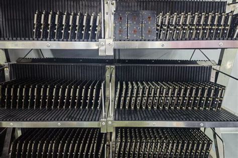
Scalable Solutions for Automated PCB Assembly
When scaling PCB manufacturing operations, automated assembly systems must adapt to fluctuating production demands without compromising precision. Modular equipment designs allow PCB manufacturing companies to incrementally expand capacity, integrating additional pick-and-place modules or conveyor systems as order volumes grow. To control PCB manufacturing cost, prioritize machines with adaptive feeders that handle diverse component sizes, reducing changeover downtime and material waste.
Advanced vision systems paired with machine learning algorithms ensure consistent placement accuracy, even at high speeds—critical for maintaining yield rates in PCB manufacturing business environments. Collaborative robotics further enhance scalability by working alongside human operators for tasks requiring nuanced inspection or complex board handling. For enterprises targeting mass production, inline testing stations embedded within the assembly line provide real-time quality feedback, preventing bottlenecks.
By aligning automation strategies with IPC-2591 (Connected Factory Exchange) standards, you create interoperable systems that streamline data flow between design, fabrication, and assembly stages. This integration minimizes manual interventions, ensuring your scaled operations meet both throughput targets and rigorous reliability requirements.
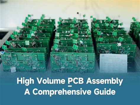
Optimizing High-Volume PCB Manufacturing Workflows
When scaling PCB manufacturing operations, streamlining workflows becomes critical to maintaining both speed and accuracy. For PCB manufacturing companies, this means adopting automated systems that reduce manual intervention while adhering to tight tolerances. Start by evaluating your material handling processes—automated conveyors and robotic pick-and-place systems can minimize bottlenecks, especially when paired with real-time monitoring tools.
Reducing PCB manufacturing cost often hinges on optimizing panel utilization and minimizing waste during depaneling. Laser-based cutting systems, for example, offer precision that preserves board integrity, even at high throughputs. Simultaneously, implementing traceability protocols ensures defects are flagged early, preventing costly rework downstream.
For a sustainable PCB manufacturing business, balance scalability with quality control. Modular equipment designs allow you to expand capacity incrementally, while IPC-compliant inspection processes maintain consistency across batches. By integrating data-driven analytics, you can identify patterns in production delays or material inefficiencies, enabling proactive adjustments. Remember: the goal isn’t just faster output—it’s building workflows that adapt seamlessly to fluctuating demand without compromising on yield rates or component reliability.
Precision Depaneling Techniques for PCBs
When managing PCB manufacturing at scale, precision depaneling becomes critical to maintaining board integrity and minimizing waste. Modern depaneling methods—such as laser cutting, router-based systems, and programmable punch tools—enable PCB manufacturing companies to separate boards with micron-level accuracy. Laser systems, for instance, reduce mechanical stress on delicate components, a key advantage for designs with fine-pitch traces or embedded sensors. Router-based solutions, while faster for thicker panels, require careful calibration to avoid microcracks that could compromise reliability.
Balancing PCB manufacturing cost with quality demands strategic equipment selection. Automated depaneling tools integrated into production lines minimize human error, ensuring consistent results across thousands of units. For high-density interconnect (HDI) boards, vacuum-based hold-down systems prevent shifting during cutting, preserving alignment. Adhering to IPC guidelines for edge smoothness and burr reduction further safeguards component performance post-depaneling.
In the PCB manufacturing business, scalability hinges on adaptable processes. Modular depaneling systems allow quick reconfiguration for varying panel sizes or material types, reducing downtime during product transitions. Pairing these techniques with real-time monitoring ensures defects are flagged early, aligning with stringent quality benchmarks while optimizing throughput. By prioritizing precision, you not only protect component functionality but also strengthen your competitive edge in high-volume markets.
Meeting IPC Standards in PCB Engineering
When scaling PCB manufacturing operations, adhering to IPC standards becomes non-negotiable for ensuring consistent quality and reliability. These guidelines govern everything from material selection to final inspections, helping PCB manufacturing companies avoid costly rework or field failures. For instance, IPC-6012 outlines acceptability criteria for rigid boards, while IPC-A-600 focuses on visual quality benchmarks. By integrating these protocols early in design, you streamline compliance checks during high-volume production phases.
A critical area is microsectioning—a process mandated by IPC-610 for evaluating plating thickness and solder joint integrity. Automated optical inspection (AOI) systems calibrated to IPC tolerances can flag deviations in real time, minimizing PCB manufacturing cost overruns caused by defects. Additionally, documentation aligned with IPC-2581 ensures traceability across supply chains, a key factor for enterprises managing global PCB manufacturing business networks.
To maintain scalability, pair IPC-compliant workflows with depaneling solutions that preserve board integrity under rapid cycling. This alignment not only meets certification requirements but also reinforces your reputation as a provider of high-reliability solutions. By prioritizing these standards, you future-proof operations against evolving industry demands while balancing precision and throughput.
High-Volume PCB Production Quality Assurance
Ensuring consistent quality in PCB manufacturing demands rigorous testing protocols and process standardization. For high-volume projects, automated optical inspection (AOI) systems become indispensable, identifying defects like soldering errors or trace misalignments at speeds matching production throughput. Leading PCB manufacturing companies integrate statistical process control (SPC) tools to monitor variability, ensuring every batch adheres to IPC Class 2 or 3 standards.
Balancing PCB manufacturing cost with reliability requires optimizing material selection and minimizing rework cycles. Advanced thermal profiling during soldering, for example, prevents warping or delamination, safeguarding component integrity across thousands of boards. To maintain scalability, traceability systems track each unit from fabrication to assembly, enabling rapid root-cause analysis if anomalies arise.
For PCB manufacturing business models targeting automation, investing in in-line testing stations reduces manual inspection bottlenecks. Pairing these with IPC-compliant microsectioning validates internal layer quality without disrupting workflow continuity. This approach not only meets certification requirements but also builds trust with clients relying on your capacity to deliver defect-free volumes consistently. By aligning quality assurance with lean manufacturing principles, you create a competitive edge in high-volume markets.

Conclusion
When scaling PCB manufacturing operations, balancing pcb manufacturing cost with uncompromising quality requires strategic precision. By integrating advanced precision depaneling systems and adhering to IPC-compliant microsectioning protocols, you ensure component integrity while meeting the demands of high-volume production. For pcb manufacturing companies, this approach not only streamlines workflows but also reduces long-term risks associated with defects or compliance gaps.
Optimizing your pcb manufacturing business hinges on adopting scalable solutions that align with automated assembly environments. Whether refining depaneling accuracy or implementing rigorous quality checks, every decision must prioritize repeatability and efficiency. Partnering with suppliers who understand high-volume tolerances and material consistency can further enhance your competitive edge.
Ultimately, success in pcb manufacturing lies in harmonizing technical precision with operational scalability. By focusing on data-driven process improvements and leveraging industry-tested standards, you position your operations to thrive in markets where reliability and speed define profitability.

FAQs
How does PCB manufacturing cost vary for high-volume projects?
High-volume PCB manufacturing typically reduces per-unit costs through economies of scale, but expenses depend on design complexity, material choices, and quality certifications. Automated depaneling and IPC-compliant microsectioning further optimize costs by minimizing waste and rework.
What should you prioritize when selecting PCB manufacturing companies?
Look for suppliers with proven expertise in high-volume PCB production, certifications like ISO 9001 or IPC Class 3, and scalable infrastructure. Ensure they integrate precision depaneling systems and rigorous testing protocols to maintain component integrity.
How do you ensure quality in a PCB manufacturing business?
Implement IPC standards for design validation, material inspection, and post-production testing. Automated optical inspection (AOI) and microsectioning analysis help identify defects early, ensuring compliance with reliability benchmarks for mission-critical applications.
Can you reduce PCB manufacturing cost without compromising quality?
Yes. Optimize panel layouts to maximize material usage, standardize designs for automated assembly, and partner with PCB manufacturing companies that offer volume-based pricing. Advanced depaneling techniques also reduce mechanical stress, lowering failure rates.
What’s critical for scaling high-volume PCB production?
Adopt modular workflows that align with automated assembly lines. Invest in depaneling systems with high throughput rates and precision tolerances. Regularly audit PCB manufacturing processes to identify bottlenecks and ensure seamless scalability.
Ready to Elevate Your PCB Production?
For tailored solutions that align with high-volume PCB manufacturing demands, please click here to explore advanced engineering strategies and cost-optimized workflows.