Single Layer PCB Board: Design, Advantages, and Applications
Introduction
Printed Circuit Boards (PCBs) are the backbone of modern electronics, providing mechanical support and electrical connections for electronic components. Among the various types of PCBs, the single-layer PCB (single-sided PCB) is the simplest and most cost-effective solution for many applications. Despite its simplicity, single-layer PCBs are widely used in consumer electronics, industrial controls, and automotive systems due to their affordability and ease of manufacturing.
This article explores the design considerations, advantages, limitations, and common applications of single-layer PCBs, providing a comprehensive understanding of their role in electronics.
What is a Single Layer PCB?
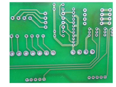
A single-layer PCB consists of a single conductive copper layer laminated onto a non-conductive substrate (typically fiberglass or phenolic resin). The electronic components are mounted on one side, while the copper traces are routed on the opposite side. Since there is only one conductive layer, the design must ensure that traces do not cross without jumpers or bridges.
Key Features of Single-Layer PCBs
- Single conductive layer (copper)
- Components mounted on one side
- Simpler and cheaper to manufacture
- Used in low-complexity circuits
Design Considerations for Single-Layer PCBs
Designing a single-layer PCB requires careful planning due to the limited routing space. Below are key considerations:
1. Component Placement
- Components should be arranged to minimize trace crossings.
- Dense component placement can lead to routing difficulties, so adequate spacing is necessary.
2. Trace Routing
- Since traces cannot cross on a single layer, jumpers or zero-ohm resistors may be needed to avoid intersections.
- Wider traces are used for high-current paths to prevent overheating.
3. Power and Ground Routing
- A solid ground plane is often impractical, so ground traces must be carefully routed.
- Star grounding helps reduce noise in analog circuits.
4. Via Alternatives
- Single-layer PCBs do not have plated through-holes (vias) for layer transitions.
- Jumper wires or through-hole component leads can serve as manual vias.
5. Design Rule Check (DRC)
- Always perform a Design Rule Check to ensure proper trace width, spacing, and manufacturability.
Advantages of Single-Layer PCBs
Single-layer PCBs offer several benefits, making them ideal for many applications:
1. Cost-Effective
- Requires less material (only one copper layer).
- Simpler manufacturing process reduces production costs.
2. Faster Prototyping and Production
- Fewer layers mean shorter fabrication time.
- Ideal for quick-turn prototypes.
3. Easier to Design and Repair
- Simpler layout reduces design complexity.
- Troubleshooting and repairs are easier due to straightforward trace routing.
4. Suitable for Low-Density Circuits
- Works well for simple analog and digital circuits (e.g., power supplies, LED drivers, relays).
5. Reliable for High-Frequency Applications
- Fewer layers reduce signal interference and crosstalk in certain cases.
Limitations of Single-Layer PCBs
Despite their advantages, single-layer PCBs have some drawbacks:
1. Limited Routing Space
- Only one conductive layer restricts complex circuit designs.
- Jumpers may be needed, increasing assembly time.
2. Not Suitable for High-Density Designs
- Complex circuits (e.g., microprocessors, multi-channel systems) require multi-layer PCBs.
3. Larger Board Size
- More space is needed to route traces without overlaps, increasing PCB dimensions.
4. Reduced Performance in High-Speed Circuits
- Lack of proper ground planes can lead to electromagnetic interference (EMI) issues.
Applications of Single-Layer PCBs
Due to their simplicity and cost-effectiveness, single-layer PCBs are used in various industries:
1. Consumer Electronics
- Remote controls
- Calculators
- LED lighting systems
2. Automotive Electronics
- Relay controllers
- Dashboard indicators
- Simple sensor modules
3. Industrial Control Systems
- Power supplies
- Motor controllers
- Timers and counters
4. Medical Devices
- Basic diagnostic equipment
- Wearable health monitors
5. Educational and DIY Projects
- Arduino-based projects
- Breadboard replacements for simple circuits
Single-Layer PCB vs. Multi-Layer PCB
| Feature | Single-Layer PCB | Multi-Layer PCB |
|---|---|---|
| Layers | 1 conductive layer | 2+ conductive layers |
| Cost | Low | High |
| Design Complexity | Simple | Complex |
| Routing Flexibility | Limited (jumpers may be needed) | High (traces can cross on different layers) |
| Size | Larger due to routing constraints | Compact due to layered routing |
| Applications | Simple circuits, low-cost devices | High-speed, high-density circuits |
Conclusion
Single-layer PCBs remain a fundamental choice for low-cost, simple electronic designs. While they lack the complexity of multi-layer boards, their affordability, ease of manufacturing, and reliability make them indispensable in consumer electronics, automotive systems, and industrial controls.
For engineers and hobbyists working on basic circuits, prototypes, or cost-sensitive projects, single-layer PCBs provide an efficient and economical solution. However, for high-speed, high-density applications, transitioning to multi-layer PCBs becomes necessary.
By understanding the design principles, advantages, and limitations of single-layer PCBs, developers can make informed decisions when selecting the right PCB type for their projects.